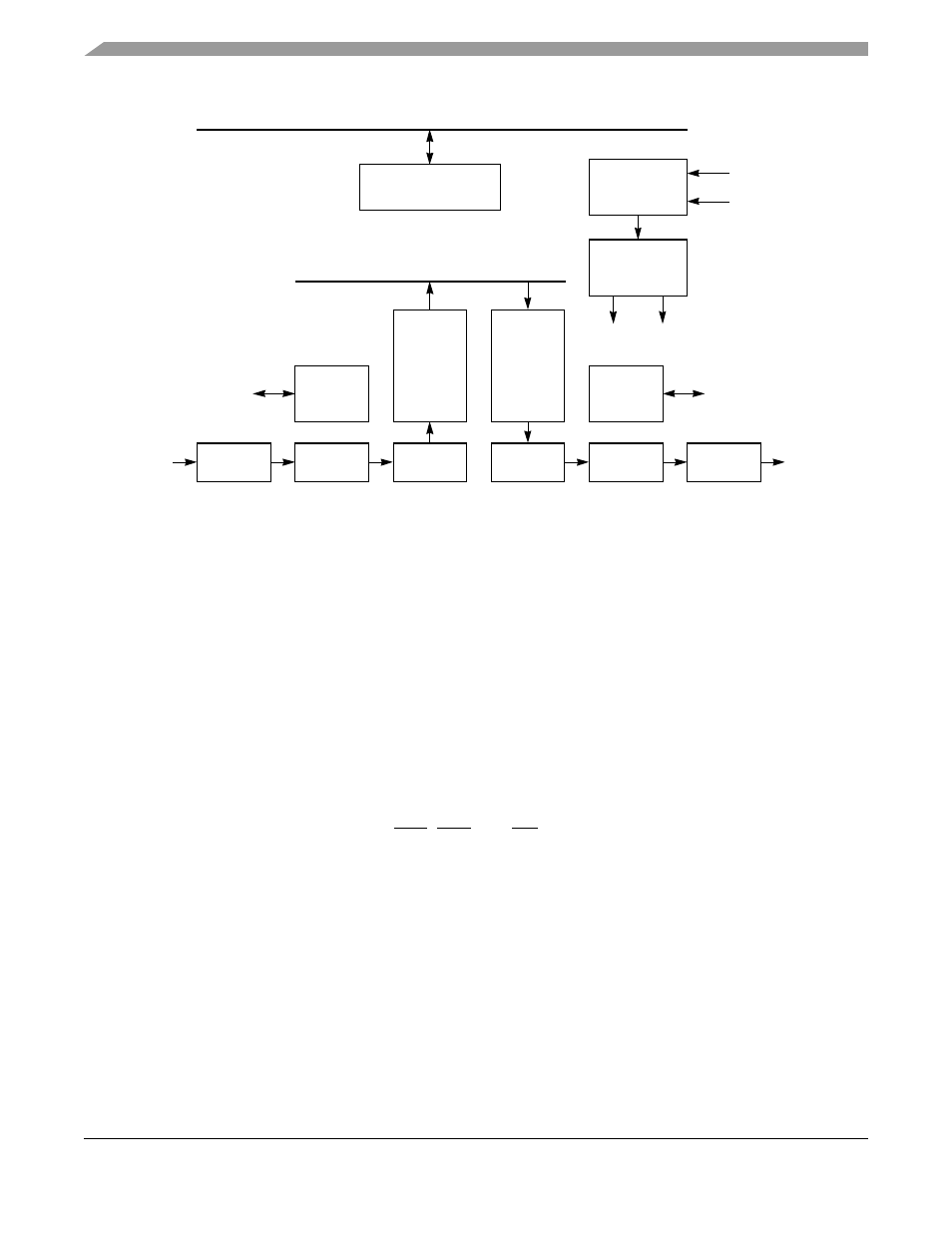
Figure 20-1. scc block diagram, 1 features, Features -2 – Freescale Semiconductor MPC8260 User Manual
Page 680: Scc block diagram -2, Figure 20-1
Serial Communications Controllers (SCCs)
MPC8260 PowerQUICC II Family Reference Manual, Rev. 2
20-2
Freescale Semiconductor
Figure 20-1. SCC Block Diagram
20.1
Features
The following is a list of the main SCC features. (Performance figures assume a 25-MHz system clock.)
•
Implements HDLC/SDLC, HDLC bus, synchronous start/stop, asynchronous start/stop (UART),
AppleTalk/LocalTalk, and totally transparent protocols
•
Supports 10-Mbps Ethernet/IEEE 802.3 (half- or full-duplex) on all SCCs
•
Additional protocols may be available through the use of RAM-based microcodes. Please contact
your Freescale sales office.
•
DPLL circuitry for clock recovery with NRZ, NRZI, FM0, FM1, Manchester, and Differential
Manchester (also known as Differential Bi-phase-L)
•
Clocks can be derived from a baud rate generator, an external pin, or DPLL
•
Data rate for asynchronous communication can be as high as 16.62 Mbps at 133 MHz
•
Supports automatic control of the RTS, CTS, and CD modem signals
•
Multi-buffer data structure for receive and send (the number of buffer descriptors (BDs) is limited
only by the size of the internal dual-port RAM—8 bytes per BD)
•
Deep FIFOs (SCC transmit and receive FIFOs are 32 bytes each.)
•
Transmit-on-demand feature decreases time to frame transmission (transmit latency)
•
Low FIFO latency option for send and receive in character-oriented and totally transparent
protocols
•
Frame preamble options
•
Full-duplex operation
Decoder
Delimiter
Shifter
Delimiter
Internal Clocks
Encoder
Modem Lines
Rx
Control
Unit
Rx
Data
FIFO
Tx
Data
FIFO
Tx
Control
Unit
RXD
Modem Lines
Clock
Generator
DPLL
and Clock
Recovery
TCLK
TXD
Control
Registers
Shifter
60x Bus
Peripheral Bus
RCLK