3 scc parameter ram, Scc parameter ram -13, Scc parameter ram map for all protocols -13 – Freescale Semiconductor MPC8260 User Manual
Page 691
Serial Communications Controllers (SCCs)
MPC8260 PowerQUICC II Family Reference Manual, Rev. 2
Freescale Semiconductor
20-13
20.3
SCC Parameter RAM
Each SCC parameter RAM area begins at the same offset from each SCC base area.
describes the SCC’s base addresses. The protocol-specific portions of the SCC
parameter RAM are discussed in the specific protocol descriptions and the part that is common to all SCC
protocols is shown in
.
Some parameter RAM values must be initialized before the SCC can be enabled. Other values are
initialized or written by the CPM. Once initialized, most parameter RAM values do not need to be accessed
because most activity centers around the descriptors rather than the parameter RAM. However, if the
parameter RAM is accessed, note the following:
•
Parameter RAM can be read at any time.
•
Tx parameter RAM can be written only when the transmitter is disabled—after a
STOP
TRANSMIT
command and before a
RESTART
TRANSMIT
command or after the buffer/frame finishes
transmitting after a
GRACEFUL
STOP
TRANSMIT
command and before a
RESTART
TRANSMIT
command.
•
Rx parameter RAM can be written only when the receiver is disabled. Note the
CLOSE
RXBD
command does not stop reception, but it does allow the user to extract data from a partially full Rx
buffer.
•
See
Section 20.3.7, “Reconfiguring the SCCs.”
shows the parameter RAM map for all SCC protocols. Boldfaced entries must be initialized by
the user.
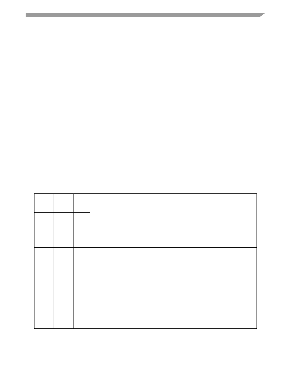
Table 20-4. SCC Parameter RAM Map for All Protocols
Offset
1
Name
Width
Description
0x00
RBASE
Hword
Rx/TxBD table base address—offset from the beginning of dual-port RAM. The BD
tables can be placed in any unused portion of the dual-port RAM. The CPM starts BD
processing at the top of the table. (The user defines the end of the BD table by setting
the W bit in the last BD to be processed.) Initialize these entries before enabling the
corresponding channel. Erratic operations occur if BD tables of active SCCs overlap.
Values in RBASE and TBASE should be multiples of eight.
0x02
TBASE
Hword
0x04
RFCR
Byte
Rx function code. See
Section 20.3.2, “Function Code Registers (RFCR and TFCR)
0x05
TFCR
Byte
Section 20.3.2, “Function Code Registers (RFCR and TFCR)
.”
0x06
MRBLR
Hword
Maximum receive buffer length. Defines the maximum number of bytes the
PowerQUICC II writes to a receive buffer before it goes to the next buffer. The
PowerQUICC II can write fewer bytes than MRBLR if a condition such as an error or
end-of-frame occurs. It never writes more bytes than the MRBLR value. Therefore,
user-supplied buffers should be no smaller than MRBLR. MRBLR should be greater than
zero for all modes. It should be a multiple of 4 for Ethernet and HDLC modes, and in
totally transparent mode unless the Rx FIFO is 8-bits wide (GSMR_H[RFW] = 1).
Note: Although MRBLR is not intended to be changed while the SCC is operating, it can
be changed dynamically in a single-cycle, 16-bit move (not two 8-bit cycles).
Changing MRBLR has no immediate effect. To guarantee the exact Rx BD on
which the change occurs, change MRBLR only while the receiver is disabled.
Transmit buffer length is programmed in TxBD[Data Length] and is not affected by
MRBLR.