Figure 32-18. cps switch rx queue descriptor, Table 32-9. cps switch rxqd field descriptions, 6 switch receive/transmit buffer descriptor (rxbd) – Freescale Semiconductor MPC8260 User Manual
Page 1092: Cps switch rx queue descriptor -30, Switch receive/transmit buffer descriptor -30, Cps switch rxqd field descriptions -30, Figure 32-19, Figure 32-18, Table 32-9 describes the cps switch rxqd fields
ATM AAL2
MPC8260 PowerQUICC II Family Reference Manual, Rev. 2
32-30
Freescale Semiconductor
describes the CPS switch RxQD fields.
32.4.4.6
SWITCH Receive/Transmit Buffer Descriptor (RxBD)
The switch buffer structure consists of a BD table that points to data buffers. The RxBDs contain, apart
from the buffer pointer, the packet header, as shown in
. The buffers contain the packet
payload. This BD is common to the receiver and the transmitter.
Table 3-11 describes the Switch RxBD fields.
0
7
8
11
12
13
14
15
Offset + 0x00
TX CID
—
RBM
PPD
SubType
Offset + 0x02
TxQD Pointer
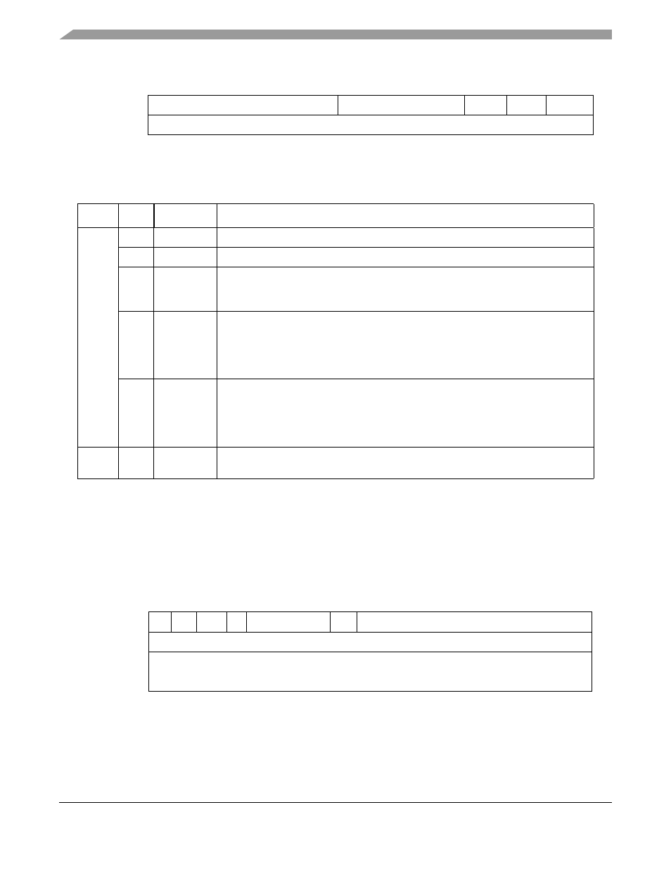
Figure 32-18. CPS Switch Rx Queue Descriptor
Table 32-9. CPS Switch RxQD Field Descriptions
Offset
Bits
Name
1
1
Boldfaced entries must be initialized by the user.
Description
0x00
0-7
TX CID
Translation CID. The received CID is saved in a TX Queue with this new CID number.
8-11
—
Reserved, should be cleared during initialization.
12
RBM
Receive buffer mask
0 Disable receive buffer interrupt
1 Enable receive buffer interrupt
13
PPD
Partial packet discard
0 Normal mode
1 When a buffer-not-ready event causes a packet to be discarded, the remainder of the
SSSAR SDU is also discarded. This allows for better performance for switched
channels that implement SSSAR.
14-15
SubType
Sublayer type. Should be 01 (CPS switched) for this descriptor.
00 CPS sublayer
01 CPS switched
10 SSSAR
11 Reserved
0x02
—
TxQD
Pointer
Points to the TxQD into which the packets of this CID are stored and later sent.
0
1
2
3
4
5
6
7
8
15
Offset + 0x00 E/R
0
W
I
—
UP
CPS Packet Header
Offset + 0x02
Packet Header (Receiver CC)
Offset + 0x04
Rx Data Buffer Pointer (RXDBPTR)
Offset + 0x06
Figure 32-19. Switch Receive/Transmit Buffer Descriptor