Freescale Semiconductor MPC8260 User Manual
Page 1040
ATM AAL1 Circuit Emulation Service
MPC8260 PowerQUICC II Family Reference Manual, Rev. 2
31-24
Freescale Semiconductor
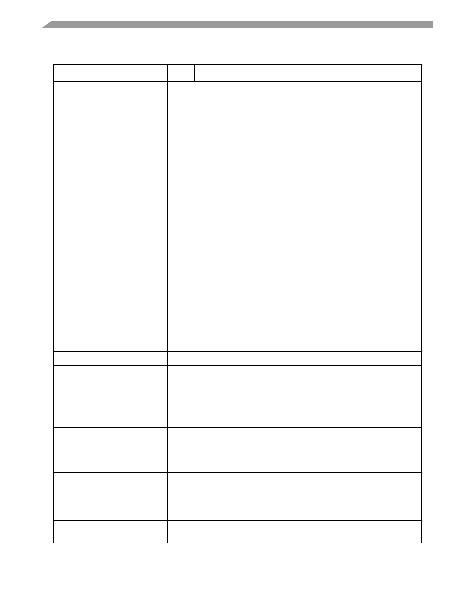
0x82
VCI_Filtering
Hword
VCI filtering enable bits. When cells with VCI = 3, 4, 6, 7-15 are received
and the associated VCI_Filtering bit = 1 the cell is sent to the raw cell
queue. VCI=3 is associated with VCI_Filtering[3], VCI=15 is associated
with VCI_Filtering[15]. VCI_Filtering[0–2, 5] should be zero. See
Section 30.10.1.2, “VCI Filtering (VCIF)
.”
0x84
GMODE
Hword
Global mode. User-defined. See
Section 30.10.1.3, “Global Mode Entry
.”
0x86
COMM_INFO
Hword
The information field associated with the last host command.
User-defined. See
Section 30.14, “ATM Transmit Command
.”
0x88
Hword
0x8A
Hword
0x8C
Reserved
Word
Reserved, should be cleared during initialization.
0x90
CRC32_PRES
Word
Preset for CRC32. Initialize to 0xFFFFFFFF.
0x94
CRC32_MASK
Word
Constant mask for CRC32. Initialize to 0xDEBB20E3.
0x98
AAL1_SNPT_BASE
Hword
AAL1 SNP protection look up table base address. (AAL1 and AAL1 CES
only.) The 32-byte table resides in dual-port RAM and must be initialized
by the user (See
Section 31.14, “AAL1 Sequence Number (SN)
.”).
0x9A
—
Hword
Reserved, should be cleared during initialization.
0x9C
SRTS_BASE
Word
External SRTS logic base address. (AAL1and AAL1 CES only.) Should
be 16-byte aligned.
0xA0
IDLE/UNASSIGN_BASE Hword
Idle/unassign cell base address. Points to dual-port RAM area contains
idle/unassign cell template (little-endian format). Should be 64-byte
aligned. User-defined. The ATM header should be 0x0000_0000 or
0x0100_0000 (CLP=1).
0xA2
IDLE/UNASSIGN_SIZE
Hword
Idle/Unassign cell size. 52 in regular mode. 53–64 in UDC mode.
0xA4
EPAYLOAD
Word
Reserved payload. Initialize to 0x6A6A6A6A.
0xA8
Trm
Word
(ABR only) The upper bound on the time between F-RM cells for an active
source. TM 4.0 defines the Trm period as 100 msec. The Trm value is
defined by the system clock and the time stamp timer prescaler (See
RTSCR). For time stamp prescalar of 1µS, Trm should be set to 100
ms/1µs = 100,000.
0xAC
Nrm
Hword
(ABR only) Controls the maximum cells the source may send for each
F-RM cell. Set to 32 cells.
0xAE
Mrm
Hword
(ABR only) Controls the bandwidth between F-RM, B-RM and user data
cell. Set to 2 cells.
0xB0
TCR
Hword
(ABR only) Tag cell rate. The minimum cell rate allowed for all ABR
channels. An ABR channel whose ACR is less then TCR sends only
out-of-rate F-RM cells at TCR. Should be set to 10 cells/sec as defined in
the TM 4.0. Uses the ATMF TM 4.0 floating-point format. Note that the
APC minimum cell rate should be at least TCR.
0xB2
ABR_RX_TCTE
Hword
(ABR only) Points to total of 16 bytes reserved dual-port RAM area used
by the CP. Should be 16 byte aligned. User-defined.
Table 31-3. AAL1 CES Field Descriptions (continued)
Offset
Name
Width
Description