Figure 27-3. smc memory structure, 3 smc parameter ram, Smc parameter ram -5 – Freescale Semiconductor MPC8260 User Manual
Page 817: Smc memory structure -5
Serial Management Controllers (SMCs)
MPC8260 PowerQUICC II Family Reference Manual, Rev. 2
Freescale Semiconductor
27-5
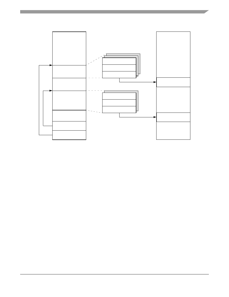
Figure 27-3. SMC Memory Structure
The BD table allows buffers to be defined for transmission and reception. Each table forms a circular
queue. The CP uses BDs to confirm reception and transmission so that the processor knows buffers have
been serviced. The data resides in external or internal buffers.
When SMCs are configured to operate in GCI mode, their memory structure is predefined to be one
half-word long for transmit and one half-word long for receive. For more information on these half-word
structures, see
Section 27.5, “The SMC in GCI Mode.”
27.2.3
SMC Parameter RAM
The CP accesses each SMC’s parameter table using a user-programmed pointer (SMCx_BASE) located in
the parameter RAM; see
Section 14.5.2, “Parameter RAM.”
Each SMC parameter RAM table can be
placed at any 64-byte aligned address in the dual-port RAM’s general-purpose area (banks 1–8, 11 and 12).
The protocol-specific portions of the SMC parameter RAM are discussed in the sections that follow. The
SMC parameter RAM shared by the UART and transparent protocols is shown in
. Parameter
RAM for GCI protocol is described in
Status and Control
Data Length
Buffer Pointer
Pointer to SMCx
TxBD Table
Pointer to SMCx
RxBD Table
SMC RxBD
Table
SMC TxBD
Table
Dual-Port RAM
Status and Control
Data Length
Buffer Pointer
Tx Data Buffer
External Memory
RxBD Table
TxBD Table
Rx Data Buffer