Risc controller configuration register (rccr -9, Figure 14-3, Rccr bit fields are descri bed in table 14-3 – Freescale Semiconductor MPC8260 User Manual
Page 557
Communications Processor Module Overview
MPC8260 PowerQUICC II Family Reference Manual, Rev. 2
Freescale Semiconductor
14-9
RCCR bit fields are described in
.
0
1
2
7
8
9
10
11
12
13
14
15
Field TIME MCCPR
1
TIMEP
DR1M DR2M DR1QP
EIE
SCD
2
DR2QP
Reset
0000_0000_0000_0000
R/W
R/W
Addr
16
19
20
21
22
23
24
25
26
27
28
29
30
31
Field
ERAM
3
EDM1 EDM2 EDM3
EDM4 DR3M DR4M DR3QP DEM12 DEM34 DR4QP
Reset
0000_0000_0000_0000
R/W
R/W
Addr
0X119C6
1
Reserved on .29
µm (HiP3) Rev A.1 and B.3 devices. See
2
Reserved on .29
µm devices. See
3
ERAM[16-18] and bIt 19 is reserved on .29
.
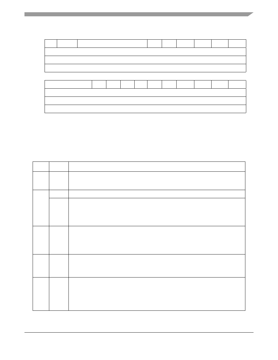
Figure 14-3. RISC Controller Configuration Register (RCCR
Table 14-3. RISC Controller Configuration Register Field Descriptions
Bits
Name Description
0
TIME
Timer enable. Enables the CP internal timer that generates a tick to the CP based on the value
programmed into the TIMEP field. TIME can be modified at any time to start or stop the scanning
of the RISC timer tables.
1
—
.29
µm (HiP3) Rev A.1 and B.3 devices: Reserved, should be cleared.
MCCPR
.29
µm (HiP3) Rev. C.2 and .25µm (HiP4) devices: MCC request priority. Controls the priority of the
MCCs in relation to the other communication peripherals. See Table13-2. “Peripheral
Prioritization,” for more information.
0 Original CPM priority scheme. MCCx priority behaves according to Table 13-2.
1 MCC priority remains at emergency level, priority level 4.
2–7
TIMEP
Timer period controls the CP timer tick. The RISC timer tables are scanned on each timer tick and
the input to the timer tick generator is the general system clock (133/166MHZ) divided by 1,024.
The formula is (TIMEP + 1)
× 1,024 = (general system clock period). Thus, a value of 0 stored in
these bits gives a timer tick of 1
× (1,024) = 1,024 general system clocks and a value of 63
(decimal) gives a timer tick of 64
× (1,024) = 65,536 general system clocks.
8, 9,
24, 25
DR
x
M
IDMA
x
request mode. Controls the IDMA request
x
(DREQ
x
) sensitivity mode. DREQ
x
is used to
activate IDMA channel
x
. See
Section 19.7, “IDMA Interface Signals
0 DREQ
x
is edge sensitive (according to EDM
x
).
1 DREQ
x
is level sensitive.
10–11,
14–15,
26–27,
30–31
DR
x
QP
IDMA
x
request priority. Controls the priority of DREQ
x
relative to the communications controllers.
Section 19.7, “IDMA Interface Signals
.”
00 DREQ
x
has more priority than the communications controllers (default).
01 DREQ
x
has less priority than the communications controllers (option 2).
10 DREQ
x
has the lowest priority (option 3).
11 Reserved