Figure 15-22. idl terminal adaptor, Table 15-9. idl signal descriptions, Idl terminal adaptor -27 – Freescale Semiconductor MPC8260 User Manual
Page 603: Idl signal descriptions -27, N in figure 15-22
Serial Interface with Time-Slot Assigner
MPC8260 PowerQUICC II Family Reference Manual, Rev. 2
Freescale Semiconductor
15-27
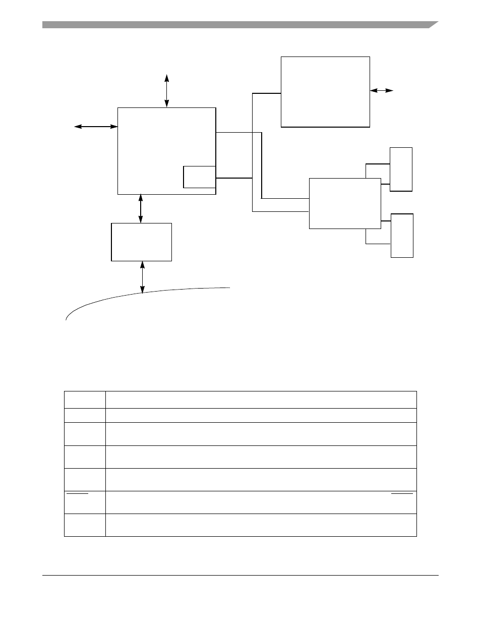
Figure 15-22. IDL Terminal Adaptor
The PowerQUICC II can identify and support each IDL channel or can output strobe lines for interfacing
devices that do not support the IDL bus. The IDL signals for each transmit and receive channel are
described in
.
Table 15-9. IDL Signal Descriptions
Signal
Description
L1RCLK
x
IDL clock; input to the PowerQUICC II.
L1RSYNC
x
IDL sync signal; input to the PowerQUICC II. This signal indicates that the clock periods following
the pulse designate the IDL frame.
L1RXD
x
IDL receive data; input to the PowerQUICC II. Valid only for the bits supported by the IDL; ignored
for any other signals present.
L1TXD
x
IDL transmit data; output from the PowerQUICC II. Valid only for the bits that are supported by the
IDL; otherwise, three-stated.
L1RQ
x
IDL request permission to transmit on the D channel; output from the PowerQUICC II on the L1RQx
pin.
L1GR
x
IDL grant permission to transmit on the D Channel; input to the PowerQUICC II on the L1TSYNCx
pin.
Note:
x
= a, b, c, and d for TDMa, TDMb, TDMc, and TDMd (for SI1 and SI2).
TSA
SCC1
Ethernet
Ethernet
PHY
LAN
ASYNC
PCM
CODEC/Filter
Monocircuit
S/T
Transceiver
SPI
ICL
(Control)
B1+B2+D
IDL
(Data)
B2+D
B1
PowerQUICC II
System Bus (ROM and RAM)
SMC1
POTS
4 wire
SCC2
SMC2
SCC3