Figure 10-4. pll filtering circuit, Pll filtering circuit -7, Figure 10-4 – Freescale Semiconductor MPC8260 User Manual
Page 413
Clocks and Power Control
MPC8260 PowerQUICC II Family Reference Manual, Rev. 2
Freescale Semiconductor
10-7
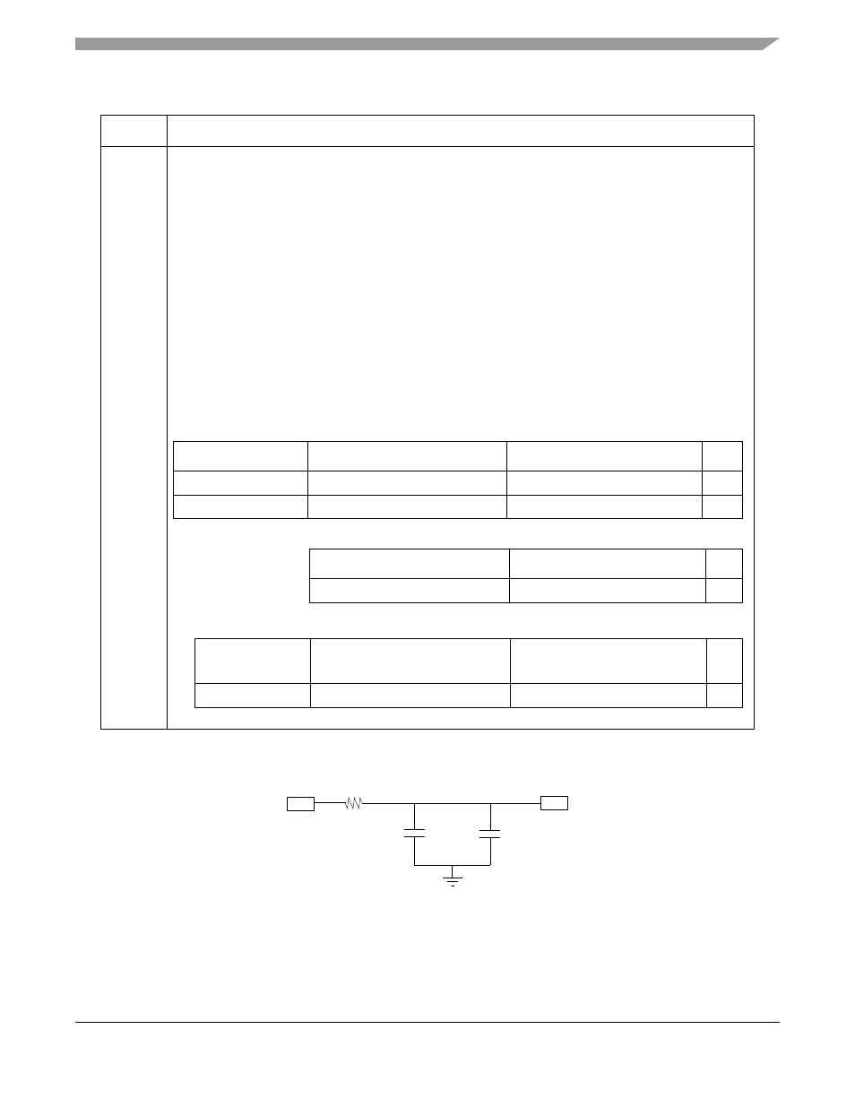
shows the filtering circuit for VCCSYN and VCCSYN1, described in
Figure 10-4. PLL Filtering Circuit
XFC
External filter capacitor—Connects to the off-chip capacitor for the main PLL filter. One terminal of the
capacitor is connected to XFC while the other terminal is connected to VCCSYN. 30 M
Ω is the minimum
parasitic resistance value that ensures proper PLL operation when connected in parallel with the XFC
capacitor. A multiplication factor (MF) based on CPM_CLK/CLKIN determines the XFC capacitor value
according to the following tables:
Definition of Multiplication Factor (MF)
If the ratio of CPM_CLK/CLKIN is an integer (A), MF = A. If CPM_CLK/CLKIN is A.5, MF = 2 x A.5. For
example, if CPM_CLK/CLKIN is 166.66 MHz/ 66.66 MHz = 2.5, then MF = 5. The relevant factors are as
follows:
CPM_CLK/CLKIN = 2
MF = 2
CPM_CLK/CLKIN = 2.5 MF = 5
CPM_CLK/CLKIN = 3 MF = 3
CPM_CLK/CLKIN = 3.5 MF = 7
CPM_CLK/CLKIN = 4
MF = 4
CPM_CLK/CLKIN = 5
MF = 5
CPM_CLK/CLKIN = 6
MF = 6
Table 10-1. Dedicated PLL Pins (continued)
Signal Description
.29
µm (HiP3) Silicon: Rev. A.1 and B.x
Multiplication Factor
Maximum Allowed Capacitance
Minimum Allowed Capacitance
Unit
MF
≤ 4
MF x 840 - 90
MF x 750 - 90
pF
MF > 4
MF x 1220
MF x 1100
pF
.29
µm (HiP3) Silicon: Rev. C.2 and Future Revisions
Maximum Allowed Capacitance
Minimum Allowed Capacitance
Unit
MF x 840 - 90
MF x 750 - 90
pF
.25
µm (HiP4) Silicon
Recommended
Capacitance
Maximum Allowed Capacitance
Minimum Allowed Capacitance
Unit
MF x 680 - 120
MF x 780 - 140
MF x 580 -100
pF
10
Ω
VDD
0.1 µF
10 µF
VCCSYN