Figure 11-43. gpcm memory device interface, Gpcm memory device interface -55, Figure 11-43 – Freescale Semiconductor MPC8260 User Manual
Page 473
Memory Controller
MPC8260 PowerQUICC II Family Reference Manual, Rev. 2
Freescale Semiconductor
11-55
Figure 11-43. GPCM Memory Device Interface
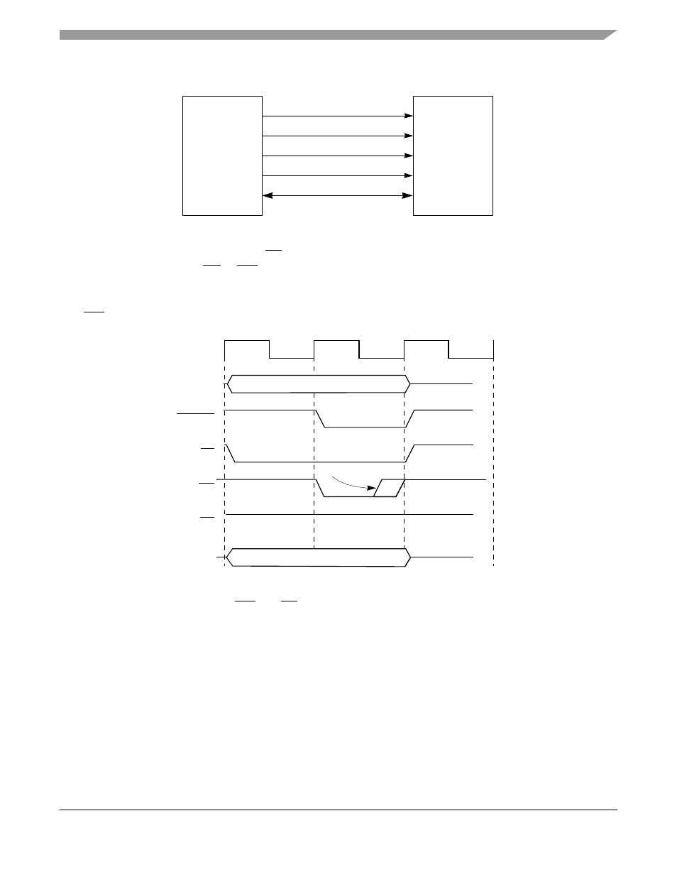
As
shows, the timing for CS is the same as for the address lines. The strobes for the
transaction are supplied by OE or WE, depending on the transaction direction (read or write). ORx[CSNT]
controls the timing for the appropriate strobe negation in write cycles. When this attribute is asserted, the
strobe is negated one quarter of a clock before the normal case. For example, when ACS = 00 and CSNT
= 1, WE is negated one quarter of a clock earlier, as shown in
.
Figure 11-44. GPCM Memory Device Basic Timing (ACS = 00, CSNT = 1, TRLX = 0)
When ACS
≠ 00 and CSNT = 1, WE and CS are negated one quarter of a clock earlier, as shown in
Address
CE
OE
W
Data
MEMORY
Data
WE
OE
CS
Address
PowerQUICC II
Clock
Address
PSDVAL
CS
WE
OE
Data
CSNT = 1