2 option registers (orx), Figure 11-7. option registers (orx)-sdram mode, Option registers (orx) -15 – Freescale Semiconductor MPC8260 User Manual
Page 433: Option registers (or x, Figure 11-7, 2 option registers (or
Memory Controller
MPC8260 PowerQUICC II Family Reference Manual, Rev. 2
Freescale Semiconductor
11-15
11.3.2
Option Registers (OR
x
)
The ORx registers define the sizes of memory banks and access attributes. The ORx attributes bits support
the following three modes of operation as defined by BR[MS].
•
SDRAM mode
•
GPCM mode
•
UPM mode
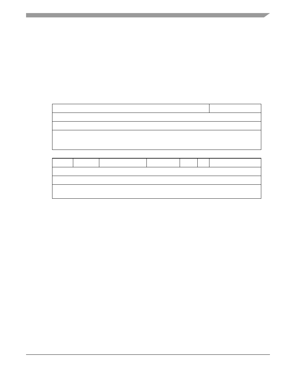
shows the ORx as it is formatted for SDRAM mode.
describes ORx fields in SDRAM mode. For more details, see
0
11
12
15
Field
SDAM
LSDAM...
Reset
0000_0000_0000_0000
1
R/W
R/W
Addr 0x0x10104 (OR0); 0x0x1010C (OR1); 0x0x10114 (OR2); 0x0x1011C (OR3); 0x0x10124 (OR4); 0x0x1012C
(OR5); 0x0x10134 (OR6); 0x0x1013C (OR7); 0x0x10144 (OR8); 0x0x1014C (OR9); 0x0x10154 (OR10);
0x0x1015C (OR11)
16
17
18
19
22
23
25
26
27
28
31
Field ...LSDAM
BPD
ROWST
NUMR
PMSEL IBID
—
Reset
0000_00000_0000_0000
1
R/W
R/W
Addr
0x10106 (OR0); 0x1010E (OR1); 0x10116 (OR2); 0x1011E (OR3); 0x10126 (OR4); 0x1012E (OR5);
0x10136 (OR6); 0x1013E (OR7); 0x10146 (OR8); 0x1014E (OR9); 0x10156 (OR10); 0x1015E (OR11)
1
Reset values are for OR0 only. OR1–11 undefined at reset.
Figure 11-7. Option Registers (OR
x)—SDRAM Mode