Table 16-5. cmxfcr field descriptions (continued), Cmx fcc clock route register (cmxfcr) -14, Cmxfcr field descriptions -14 – Freescale Semiconductor MPC8260 User Manual
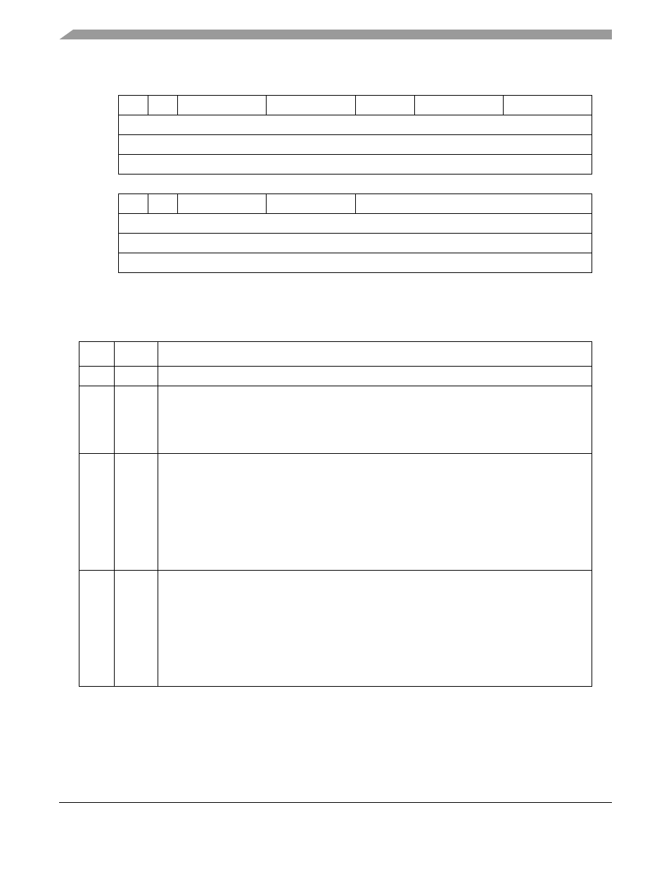
Page 624: Figure 16-10, Table 16-5 describes cmxfcr fields
CPM Multiplexing
MPC8260 PowerQUICC II Family Reference Manual, Rev. 2
16-14
Freescale Semiconductor
describes CMXFCR fields.
0
1
2
4
5
7
8
9
10
12
13
15
Field
—
FC1
RF1CS
TF1CS
FC2
RF2CS
TF2CS
Reset
0000_0000_0000_0000
R/W
R/W
Addr
16
17
18
20
21
23
24
31
Field
—
FC3
RF3CS
TF3CS
—
Reset
0000_0000_0000_0000
R/W
R/W
Addr
0x11B06
Figure 16-10. CMX FCC Clock Route Register (CMXFCR)
Table 16-5. CMXFCR Field Descriptions
Bits
Name Description
0
—
Reserved, should be cleared
1
FC1
Defines the FCC1 connection
0 FCC1 is not connected to the TSA and is either connected directly to the NMSIx pins or is not
used. The choice of general-purpose I/O port pins versus FCCn pins is made in the parallel I/O
control register.
1 FCC1 is connected to the TSA of the SIs. The NMSIx pins are available for other purposes.
2–4
RF1CS Receive FCC1 clock source (NMSI mode). Ignored if FCC1 is connected to the TSA (FC1 = 1).
000 FCC1 receive clock is BRG5.
001 FCC1 receive clock is BRG6.
010 FCC1 receive clock is BRG7.
011 FCC1 receive clock is BRG8.
100 FCC1 receive clock is CLK9.
101 FCC1 receive clock is CLK10.
110 FCC1 receive clock is CLK11.
111 FCC1 receive clock is CLK12.
5–7
TF1CS
Transmit FCC1 clock source (NMSI mode). Ignored if FCC1 is connected to the TSA (FC1 = 1).
000 FCC1 transmit clock is BRG5.
001 FCC1 transmit clock is BRG6.
010 FCC1 transmit clock is BRG7.
011 FCC1 transmit clock is BRG8.
100 FCC1 transmit clock is CLK9.
101 FCC1 transmit clock is CLK10.
110 FCC1 transmit clock is CLK11.
111 FCC1 transmit clock is CLK12.