Figure 18-6. timer reference registers (trr1-trr4), 5 timer capture registers (tcr1-tcr4), Figure 18-7. timer capture registers (tcr1-tcr4) – Freescale Semiconductor MPC8260 User Manual
Page 643: 6 timer counters (tcn1-tcn4), Figure 18-8. timer counter registers (tcn1-tcn4), 7 timer event registers (ter1-ter4), Timer capture registers (tcr1–tcr4) -7, Timer counters (tcn1–tcn4) -7, Timer event registers (ter1–ter4) -7, Timer reference registers (trr1–trr4) -7
Timers
MPC8260 PowerQUICC II Family Reference Manual, Rev. 2
Freescale Semiconductor
18-7
18.2.5
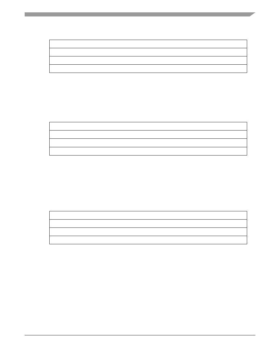
Timer Capture Registers (TCR1–TCR4)
Each timer capture register (TCR1–TCR4), shown in
, is used to latch the value of the counter
according to TMRx[CE].
18.2.6
Timer Counters (TCN1–TCN4)
Each timer counter register (TCN1–TCN4), shown in
, is an up-counter. A read cycle to TCNx
yields the current value of the timer but does not affect the counting operation. A write cycle to TCNx sets
the register to the written value, thus causing its corresponding prescaler, TMRx[PS], to be reset.
Note that the counter registers may not be updated correctly if a write is made while the timer is not
running. Use TRRx to define the preferred count value.
18.2.7
Timer Event Registers (TER1–TER4)
Each timer event register (TERx), shown in
, reports events recognized by the timers. When
an output reference event is recognized, the timer sets TERx[REF] regardless of the corresponding
TMRx[ORI]. The capture event is set only if it is enabled by TMRx[CE]. TER1–TER4 can be read at any
time.
0
15
Field
Timeout reference value
Reset
0xFFFF
R/W
R/W
Addr
0x0x10D94 (TRR1), 0x0x10D96 (TRR2), 0x0x10DA4 (TRR3), 0x0x10DA6 (TRR4)
Figure 18-6. Timer Reference Registers (TRR1–TRR4)
0
15
Field
Latched counter value
Reset
0x0000
R/W
R/W
Addr
0x0x10D98 (TCR1), 0x0x10D9A (TCR2), 0x0x10DA8 (TCR3), 0x0x10DAA (TCR4)
Figure 18-7. Timer Capture Registers (TCR1–TCR4)
0
15
Field
Up counter
Reset
0x0000
R/W
R/W
Addr
0x0x10D9C (TCN1), 0x0x10D9E (TCN2), 0x0x10DAC (TCN3), 0x0x10DAE (TCN4)
Figure 18-8. Timer Counter Registers (TCN1–TCN4)