Table 20-5. parameter ram-scc base addresses, 2 function code registers (rfcr and tfcr), Table 20-6. rfcrx /tfcrx field descriptions – Freescale Semiconductor MPC8260 User Manual
Page 693: Function code registers (rfcr and tfcr) -15, Parameter ram—scc base addresses -15, Rfcrx /tfcrx field descriptions -15, Table 20-5
Serial Communications Controllers (SCCs)
MPC8260 PowerQUICC II Family Reference Manual, Rev. 2
Freescale Semiconductor
20-15
20.3.2
Function Code Registers (RFCR and TFCR)
There are eight separate function code registers for the four SCC channels, four for Rx buffers
(RFCR1–RFCR4) and four for Tx buffers (TFCR1–TFCR4). The function code registers contain the
transaction specification associated with SDMA channel accesses to external memory.
shows
the register format.
describes RFCRx/TFCRx fields.
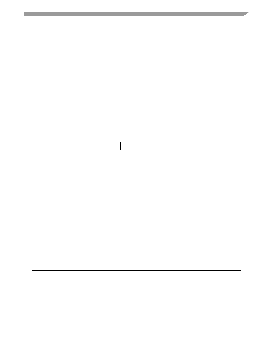
Table 20-5. Parameter RAM—SCC Base Addresses
Page
Address
1
1
Offset from RAM_Base
Peripheral
Size (Bytes)
1
0x8000 SCC1
256
2
0x8100
SCC2 256
3
0x8200
SCC3
256
4
0x8300
SCC4
256
0
1
2
3
4
5
6
7
Field
—
GBL
BO
TC2
DTB
—
Reset
0000_0000_0000_0000
R/W
R/W
Addr
SCC
x
base + 0x04 (RFCR
x
); SCC
x
base + 0x05 (TFCR
x
)
Figure 20-8. Function Code Registers (RFCR and TFCR)
Table 20-6. RFCR
x /TFCRx Field Descriptions
Bits
Name
Description
0–1
—
Reserved, should be cleared.
2
GBL
Global
0 Snooping disabled.
1 Snooping enabled.
3–4
BO
Byte ordering. Set BO to select the required byte ordering for the buffer. If BO is changed on-the-fly,
it takes effect at the beginning of the next frame (Ethernet, HDLC, and transparent) or at the
beginning of the next BD.
00 Reserved
01 Munged little-endian.
1x Big-endian or true little-endian.
5
TC2
Transfer code. Contains the transfer code value of TC[2], used during this SDMA channel memory
access. TC[0–1] is driven with a 0b11 to identify this SDMA channel access as a DMA-type access.
6
DTB
Data bus indicator
0 Use 60x bus for SDMA operation
1 Use local bus for SDMA operation
7
—
Reserved, should be cleared.