Figure 11-8. orx -gpcm mode, Or x, Orx—gpcm mode field descriptions -17 – Freescale Semiconductor MPC8260 User Manual
Page 435
Memory Controller
MPC8260 PowerQUICC II Family Reference Manual, Rev. 2
Freescale Semiconductor
11-17
shows ORx as it is formatted for GPCM mode.
describes ORx fields in GPCM mode.
26
PMSEL
Page mode select. Selects page mode for the SDRAM connected to the memory controller
bank.
0 Back-to-back page mode (normal operation). Page is closed when the bus becomes
idle.
1 Page is kept open until a page miss or refresh occurs.
27
IBID
Internal bank interleaving within same device disable. Setting this bit disables bank
interleaving between internal banks of a SDRAM device connected to the chip-select line.
IBID should be set in 60x-compatible mode if the SDRAM device is not connected to the
BANKSEL pins.
28–31
—
Reserved, should be cleared.
0
15
Field
AM
Reset
1
1111_1110_0000_0000
1
R/W
R/W
Addr 0x0x10104 (OR0); 0x0x1010C (OR1); 0x0x10114 (OR2); 0x0x1011C (OR3); 0x0x10124 (OR4); 0x0x1012C
(OR5); 0x0x10134 (OR6); 0x0x1013C (OR7); 0x0x10144 (OR8); 0x0x1014C (OR9); 0x0x10154 (OR10);
0x0x1015C (OR11)
16
17
18
19
20
21
22
23
24
27
28
29
30
31
Field AM
—
BCTLD CSNT
ACS
—
SCY
SETA TRLX EHTR
—
Reset
1
0
00
0
1
11
0
1111
0
1
0
0
R/W
R/W
Addr
0x10106 (OR0); 0x1010E (OR1); 0x10116 (OR2); 0x1011E (OR3); 0x10126 (OR4); 0x1012E (OR5);
0x10136 (OR6); 0x1013E (OR7); 0x10146 (OR8); 0x1014E (OR9); 0x10156 (OR10); 0x1015E (OR11)
1
Reset values are for OR0 only. OR1–11 are undefined at reset.
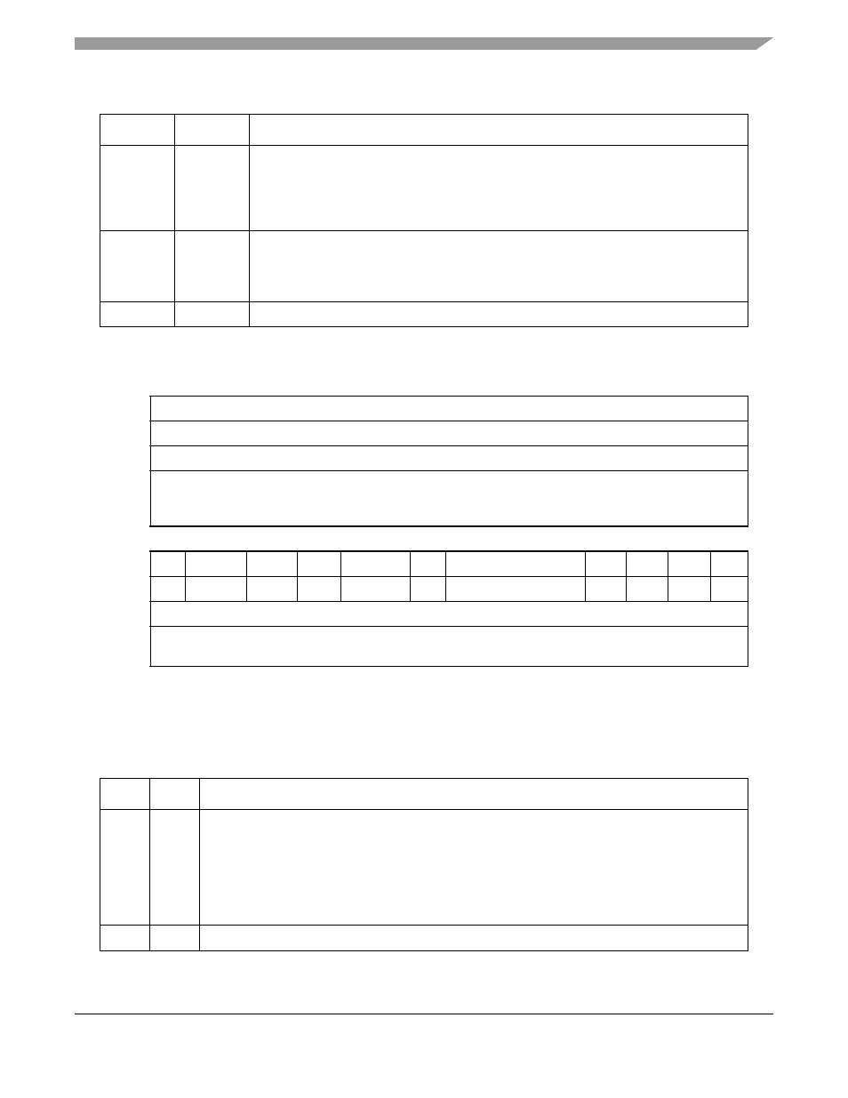
Figure 11-8. OR
x —GPCM Mode
Table 11-6. OR
x—GPCM Mode Field Descriptions
Bits
Name
Description
0–16
AM
Address mask. Masks corresponding BR
x
bits. Masking address bits independently allows external
devices of different size address ranges to be used.
0 Corresponding address bits are masked.
1 The corresponding address bits are used in the comparison with address pins. Address mask bits
can be set or cleared in any order in the field, allowing a resource to reside in more than one area
of the address map. AM can be read or written at any time.
Note: After system reset, OR0[AM] is 1111_1110_0000_0000_0.
17–18
—
Reserved, should be cleared.
Table 11-5. OR
x Field Descriptions (SDRAM Mode) (continued)
Bits
Name
Description