1 base registers (brx), Figure 11-6. base registers (brx), Table 11-4. brx field descriptions (continued) – Freescale Semiconductor MPC8260 User Manual
Page 431: Base registers (br x, Base registers (br, Brx field descriptions -13, Figure 11-6, Section 11.3.1, “base registers (brx), 1 base registers (br
Memory Controller
MPC8260 PowerQUICC II Family Reference Manual, Rev. 2
Freescale Semiconductor
11-13
11.3.1
Base Registers (BR
x
)
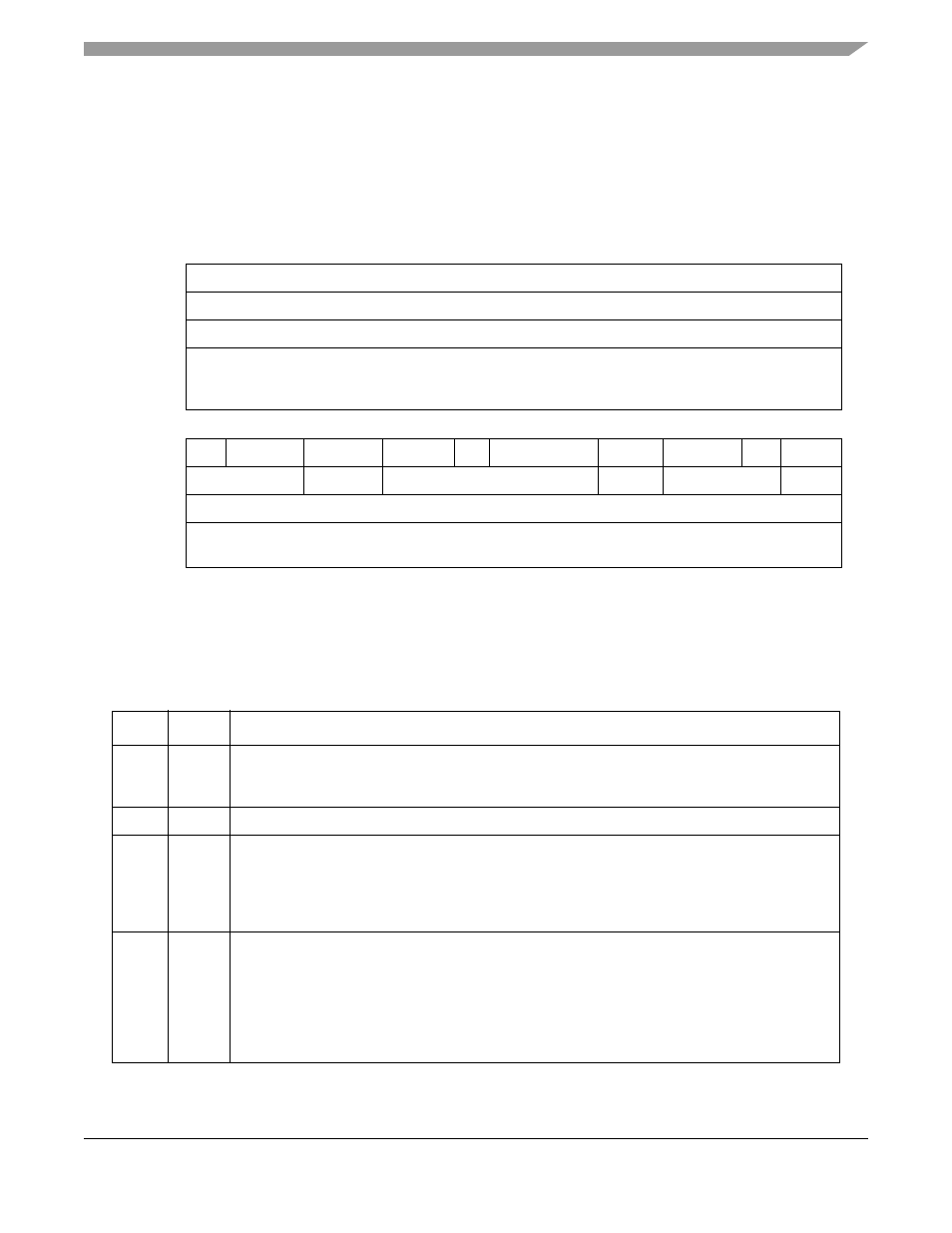
The base registers (BR0–BR11) contain the base address and address types that the memory controller uses
to compare the address bus value with the current address accessed. Each register also includes a memory
attribute and selects the machine for memory operation handling.
shows the BRx register
format.
describes BRx fields.
0
15
Field
BA
Reset
0000_0000_0000_0000
R/W
R/W
Addr 0x0x10100 (BR0); 0x0x10108 (BR1); 0x0x10110 (BR2); 0x0x10118 (BR3); 0x0x10120 (BR4); 0x0x10128
(BR5); 0x0x10130 (BR6); 0x0x10138 (BR7); 0x0x10140 (BR8); 0x0x10148 (BR9); 0x0x10150 (BR10);
0x0x10158 (BR11)
16
17
18
19
20
21
22
23
24
26
27
28
29
30
31
Field
BA
—
PS
1
DECC
WP
MS
EMEMC
1
ATOM
DR
V
1
Reset
000
see note
0000_000
see note
000
see note
R/W
R/W
Addr
0x10102 (BR0); 0x1010A (BR1); 0x10112 (BR2); 0x1011A (BR3); 0x10122 (BR4); 0x1012A (BR5);
0x10132 (BR6); 0x1013A (BR7); 0x10142 (BR8); 0x1014A (BR9); 0x10152 (BR10); 0x1015A (BR11)
1
For BR0 these fields depend on reset configuration sequence. See
Section 5.4.1, “Hard Reset Configuration Word
.”
For BR1–11, these fields are cleared at reset.
Figure 11-6. Base Registers (BR
x)
Table 11-4. BR
x Field Descriptions
Bits
Name
Description
0–16
BA
Base address. The upper 17 bits of each base address register are compared to the address on
the address bus to determine if the bus master is accessing a memory bank controlled by the
memory controller. Used with OR
x
[BSIZE].
17–18
—
Reserved, should be cleared.
19–20
PS
Port size. Specifies the port size of this memory region.
01 8-bit
10 16-bit
11 32-bit
00 64-bit (60x bus only)
21–22
DECC
Data error correction and checking. Specifies the method for data error checking and correction.
See
Section 11.2.3, “Error Checking and Correction (ECC)
Section 11.2.4, “Parity Generation
.”
00 Data errors checking disabled
01 Normal parity checking
10 Read-modify-write parity checking
11 ECC correction and checking