6 digital phase-locked loop (dpll) operation, Figure 20-13. dpll receiver block diagram, Digital phase-locked loop (dpll) operation -21 – Freescale Semiconductor MPC8260 User Manual
Page 699: Dpll receiver block diagram -21
Serial Communications Controllers (SCCs)
MPC8260 PowerQUICC II Family Reference Manual, Rev. 2
Freescale Semiconductor
20-21
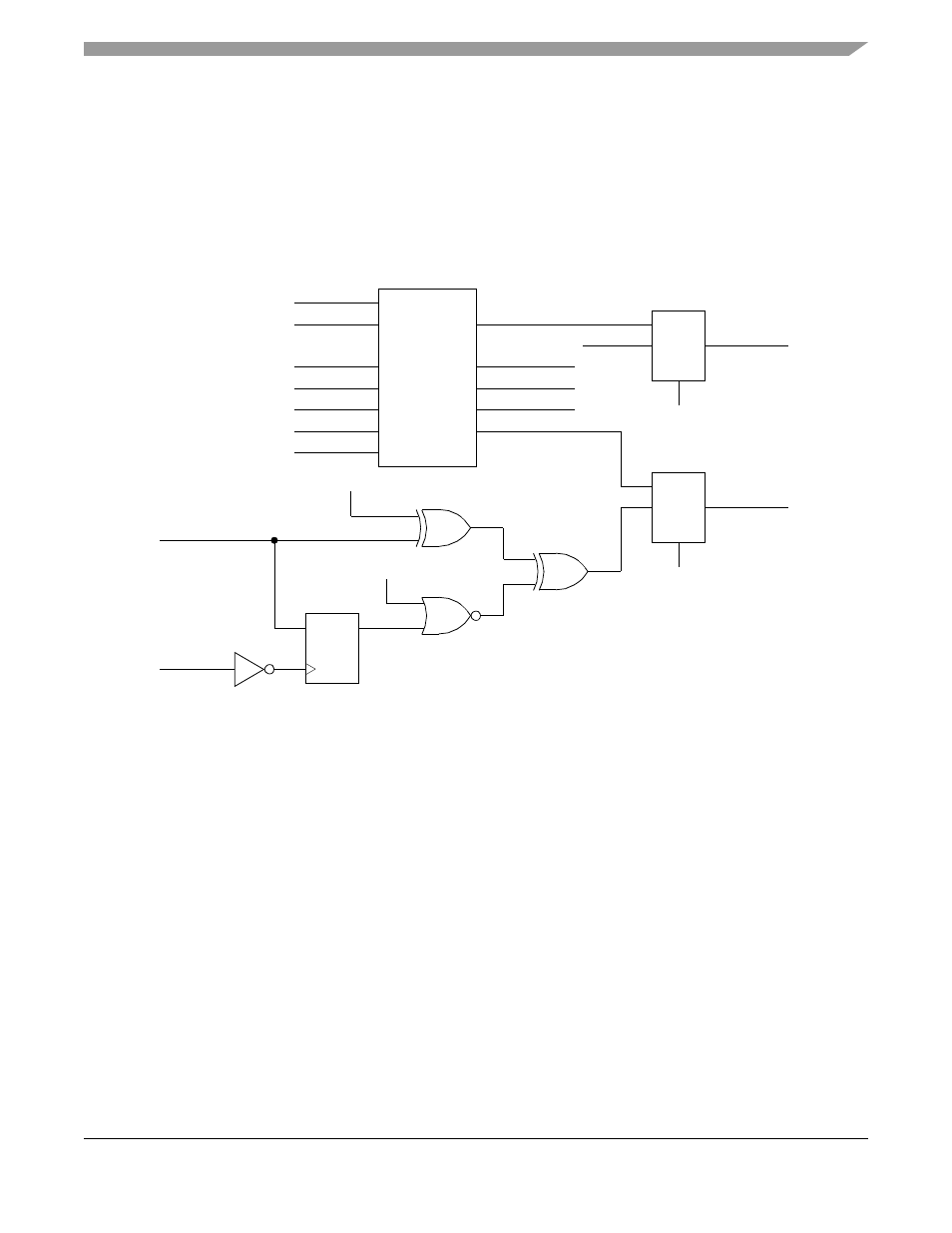
20.3.6
Digital Phase-Locked Loop (DPLL) Operation
Each SCC channel includes a digital phase-locked loop (DPLL) for recovering clock information from a
received data stream. For applications that provide a direct clock source to the SCC, the DPLL can be
bypassed by selecting 1x mode for GSMR_L[RDCR, TDCR]. If the DPLL is bypassed, only NRZ or
NRZI encodings are available. The DPLL must not be used when an SCC is programmed to Ethernet and
is optional for other protocols.
shows the DPLL receiver block;
shows the
transmitter block diagram.
Figure 20-13. DPLL Receiver Block Diagram
DPLL
HSRCLK
RXD
RINV
TSNC
EDGE
RDCR
RENC
Receiver
Carrier SNC
Decoded Data
Hunting
Noise
0
S
Recovered Clock
HSRCLK
RCLK
1
1x Mode
0
S
SCCR Data
1
1x Mode
D
CLK
Q
HSRCLK
RXD
RINV
RENC
= NRZI