1 features, Features -2, Cpm multiplexing logic (cmx) block diagram -2 – Freescale Semiconductor MPC8260 User Manual
Page 612
CPM Multiplexing
MPC8260 PowerQUICC II Family Reference Manual, Rev. 2
16-2
Freescale Semiconductor
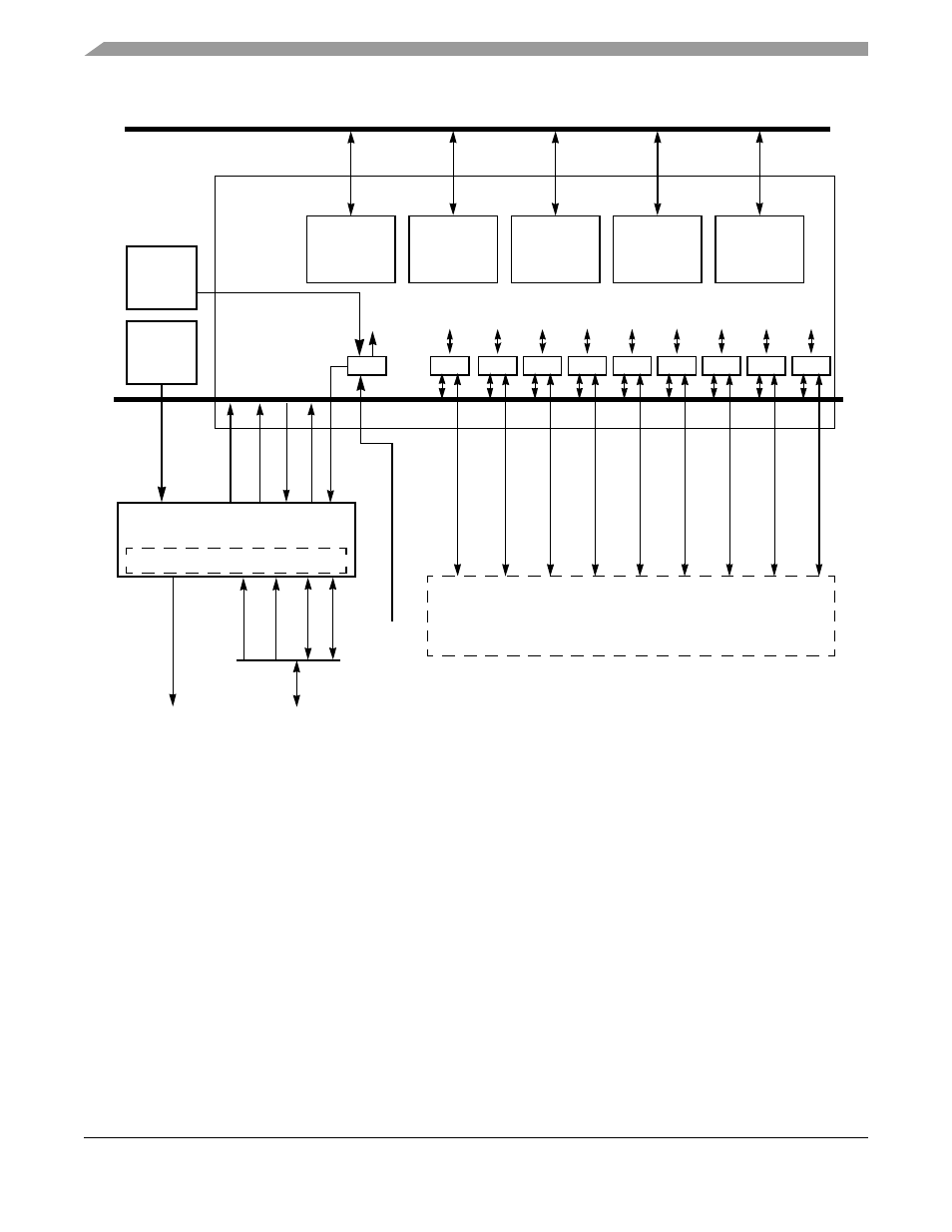
Figure 16-1. CPM Multiplexing Logic (CMX) Block Diagram
16.1
Features
The NMSI mode supports the following:
•
Each FCC, SCC, and SMC can be programmed independently to work with a serial device’s own
set of pins in a non-multiplexed manner.
•
Each FCC can be connected to its own MII (media-independent interface).
•
FCC1 can also be connected to an 8- or 16-bit ATM UTOPIA level-2 interface (not on the
MPC8250).
•
FCC2 can also be connected also to an 8-bit ATM UTOPIA level-2 interface (not on the
MPC8250).
•
FCC2 can also be connected also to the TC layer (MPC8264 and MPC8266 only).
Time-Slot Assigner
SI
x
R c
loc
k
s
T cl
ock
s
R s
y
nc
T syn
c
TDM A
x
, B
x
, C
x
, D
x
Pins
Strobes
Register Bus
TDM A
x
, B
x
, C
x
, D
x
Tx
Tx
SMC1
Nonmultiplexed Serial Interface (NMSI) Pins
Rx
Rx
Clocks
CPM MUX
BRGs
To Serials:
UTOPIA
Address
Register
2
(CMXUAR)
SMC
Clock
Register
(CMXSMR)
SCC
Clock
Register
(CMXSCR)
FCC
Clock
Register
(CMXFCR)
SI
x
Clock
Registers
(CMXSI
x
CR)
SMC1
MCCs
MUX
MII3
FCC3
MUX
MII2/
FCC2
MUX
MII1/
FCC1
MUX
SCC4
SCC4
MUX
SCC3
SCC3
MUX
SCC2
SCC2
MUX
SCC1
SCC1
MUX
SMC2
SMC2
MUX
UTOPIA
8/16
2
UTOPIA
8
2
MUX
TC Layer
1
(Option for FCC2 Only)
Note:
1
MPC8264 and MPC8266 only.
2
Not on MPC8250.