Chapter 38 serial peripheral interface (spi), Figure 38-1. spi block diagram, 1 features – Freescale Semiconductor MPC8260 User Manual
Page 1247: Serial peripheral interface (spi), Chapter 38, Features -1, Spi block diagram -1, Chapter 38, “serial peripheral interface (spi)
MPC8260 PowerQUICC II Family Reference Manual, Rev. 2
Freescale Semiconductor
38-1
Chapter 38
Serial Peripheral Interface (SPI)
The serial peripheral interface (SPI) allows the PowerQUICC II to exchange data between other
PowerQUICC II chips, the MPC860, the MC68360, the MC68302, the M68HC11 and M68HC05
microcontroller families, and peripheral devices such as EEPROMs, real-time clocks, A/D converters, and
ISDN devices.
The SPI is a full-duplex, synchronous, character-oriented channel that supports a four-wire interface
(receive, transmit, clock and slave select). The SPI block consists of transmitter and receiver sections, an
independent baud-rate generator, and a control unit. The transmitter and receiver sections use the same
clock, which is derived from the SPI baud rate generator in master mode and generated externally in slave
mode. During an SPI transfer, data is sent and received simultaneously.
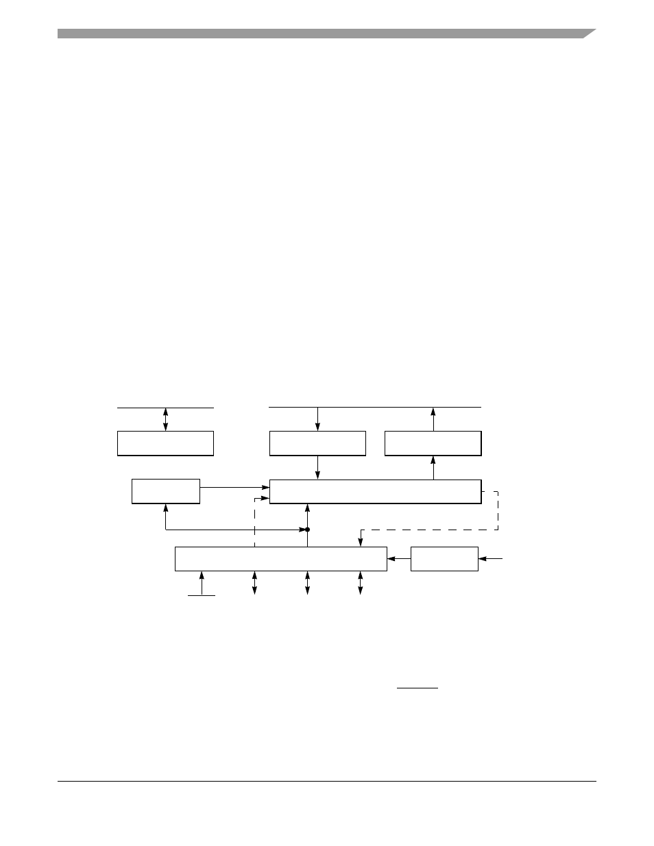
Because the SPI receiver and transmitter are double-buffered, as shown in
, the effective FIFO
size (latency) is 2 characters. The SPI’s msb is shifted out first. When the SPI is disabled in the SPI mode
register (SPMODE[EN] = 0), it consumes little power.
Figure 38-1. SPI Block Diagram
38.1
Features
The following is a list of the SPI’s main features:
•
Four-signal interface (SPIMOSI, SPIMISO, SPICLK, and SPISEL) multiplexed with port D
signals
•
Full-duplex operation
SPI Mode Register
Transmit_Register
Receive_Register
Counter
Shift_Register
SPIBRG
Pins Interface
BRGCLK
SPIMOSI
SPISEL
SPIMISO
SPICLK
TxD
RxD
IN_CLK
60x Bus
Peripheral Bus