Freescale Semiconductor MPC8260 User Manual
Page 1296
Parallel I/O Ports
MPC8260 PowerQUICC II Family Reference Manual, Rev. 2
40-18
Freescale Semiconductor
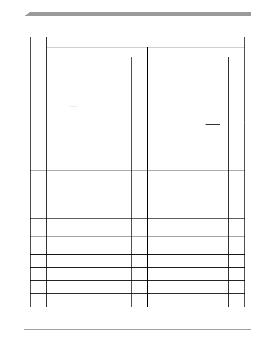
PD21
SCC4: TXD
FCC1: RxD[3]
1
UTOPIA 16
GND
TDM_A2: L1RXD
4
Inout, serial
TDM_A2:
L1RXD[0]
4
Input, nibble
(secondary option)
GND
PD20
SCC4: RTS
SCC4: TENA
Ethernet
FCC1: RxD[2]
1
UTOPIA 16
GND
TDM_A2:
L1RSYNC
4
(secondary option)
GND
PD19
FCC1: TxAddr[4]
1,
2
MPHY, master,
multiplexed polling
FCC2: TxAddr[3]
1
MPHY, master,
multiplexed polling
FCC1: TxAddr[4] 1
1,3
MPHY, slave,
multiplexed polling
FCC1: TxClav3
1,3
MPHY, master, direct
polling
FCC2: TxAddr[0]
1
MPHY, slave,
multiplexed polling
GND
BRG1: BRGO
SPI: SPISEL
(primary option)
5
V
DD
PD18
FCC1: RxAddr[4]
1,2
MPHY, master,
multiplexed polling
FCC2: RxAddr[3]
1
MPHY, master,
multiplexed polling
FCC1: RxAddr[4]
1,3
MPHY, slave,
multiplexed polling
FCC1: RxClav3
1,3
MPHY, master, direct
polling
FCC2: RxAddr[0]
1
MPHY, slave,
multiplexed polling
GND
SPI: SPICLK
Inout
(primary option)
5
GND
PD17
BRG2: BRGO
FCC1: RxPrty
UTOPIA
(primary option)
5
GND
SPI: SPIMOSI
Inout
V
DD
PD16
FCC1: TxPrty
1
UTOPIA
(primary option)
5
TDM_C1:
L1TSYNC/GRANT
4
(secondary option)
GND
SPI: SPIMISO
Inout
SPIMO
SI
PD15
TDM_C2: L1RQ
FCC1: RxD[1]
1
UTOPIA 16
GND
I2C: I2CSDA
Inout
V
DD
PD14
TDM_C2: L1CLKO
FCC1: RxD[0]
1
UTOPIA 16
GND
I2C: I2CSCL
Inout
GND
PD13
SI1: L1ST1
TDM_B1: L1TXD
Inout
GND
PD12
SI1: L1ST2
TDM_B1: L1RXD
Inout
GND
Table 40-8. Port D Dedicated Pin Assignment (PPARD = 1) (continued)
Pin
Pin Function
PSORD = 0
PSORD = 1
PDIRD = 1 (Output)
PDIRD = 0 (Input)
Defaul
t Input
PDIRD = 1 (Output)
PDIRD = 0 (Input, or
Inout if Specified)
Defaul
t Input