Figure 15-1. si block diagram, Si block diagram -2 – Freescale Semiconductor MPC8260 User Manual
Page 578
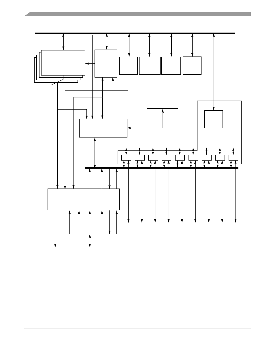
Serial Interface with Time-Slot Assigner
MPC8260 PowerQUICC II Family Reference Manual, Rev. 2
15-2
Freescale Semiconductor
Figure 15-1. SI Block Diagram
If the TSA is not used as intended, it can be used to generate complex wave forms on dedicated output
pins. For instance, it can program these pins to implement stepper motor control or variable-duty cycle and
period control on-the-fly.
Time-Slot
Assigner (TSA)
R
c
lo
cks
T cl
o
cks
R
c
lo
cks
T cl
ocks
R
sync
T s
y
nc
TDM A, B, C, D
Pins
Strobes
Route
SI RAM
Tx/Rx
RAM
Control
Mode
Register
TDM A, B, C, D
Tx
TX
Command
Register
Status
Register
SMC1 SMC2 SCC1 SCC2 SCC3 SCC4 MII1/
MII2/
MUX
MII3
To: SMC1 SMC2 SCC1 SCC2 SCC3 SCC4 FCC1 FCC2 FCC3
Multi-Channel
Peripheral Bus
Nonmultiplexed Serial Interface (NMSI) Pins
Channel #
Controllers
Shadow
Register
Clock
Route
RAM
Address
Rx
Rx
UTOPIA UTOPIA
16
1
8
1
CPM Mux
MUX
MUX
MUX
MUX
MUX
MUX
MUX
MUX
(MCCs)
Notes
The CPM mux and the MCCs are not part of the SI. (See their chapters for details.)
1
Not available on the MPC8250.