1 smc function code registers (rfcr/tfcr), Table 27-3. rfcr/tfcr field descriptions, 4 disabling smcs on-the-fly – Freescale Semiconductor MPC8260 User Manual
Page 820: Smc function code registers (rfcr/tfcr) -8, Disabling smcs on-the-fly -8, Rfcr/tfcr field descriptions -8
Serial Management Controllers (SMCs)
MPC8260 PowerQUICC II Family Reference Manual, Rev. 2
27-8
Freescale Semiconductor
27.2.3.1
SMC Function Code Registers (RFCR/TFCR)
The function code registers contain the transaction specification associated with SDMA channel accesses
to external memory.
shows the register format.
describes FCR fields.
27.2.4
Disabling SMCs On-the-Fly
An SMC can be disabled and reenabled later by ensuring that buffers are closed properly and new data is
transferred to or from a new buffer. Such a sequence is required if the parameters to be changed are not
dynamic. If the register or bit description states that dynamic changes are allowed, the sequences need not
be followed and the register or bits may be changed immediately.
NOTE
The SMC does not have to be fully disabled for parameter RAM to be
modified.
describes when parameter RAM values can be
modified. To disable all SCCs, SMCs, the SPI, and the I
2
C, use the CPCR
to reset the CPM with a single command.
0
1
2
3
4
5
6
7
Field
GBL
BO
TC2
DTB
—
R/W
R/W
Addr
SMC base + 0x04 (RFCR)/SMC base + 0x05 (TFCR)
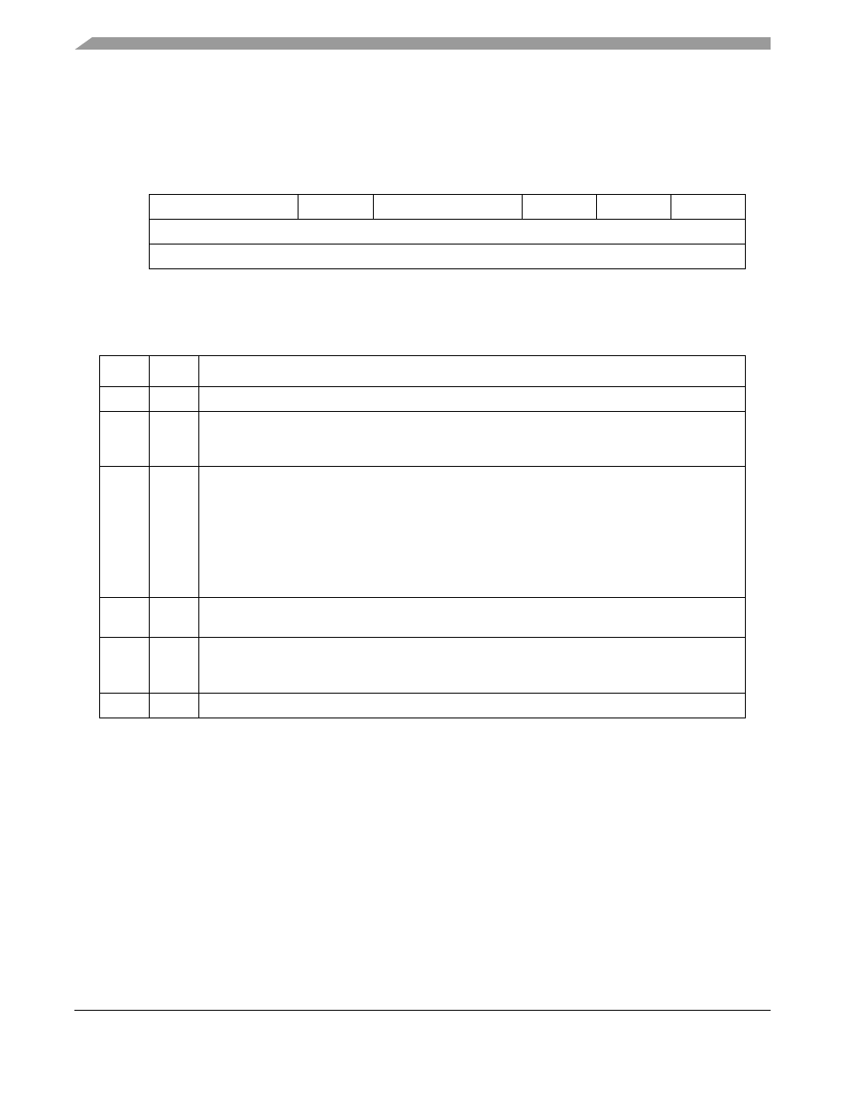
Figure 27-4. SMC Function Code Registers (RFCR/TFCR)
Table 27-3. RFCR/TFCR Field Descriptions
Bit
Name
Description
0–1
—
Reserved, should be cleared.
2
GBL
Global access bit
0 Disable memory snooping
1 Enable memory snooping
3–4
BO
Byte ordering. Selects byte ordering of the data buffer.
00 The DEC/Intel convention (swapped operation or little-endian). The transmission order of bytes
within a buffer word is opposite of Freescale mode. (32-bit port size memory only).
01 Munged little-endian. As data is sent onto the serial line from the buffer, the LSB of the buffer
double word contains data to be sent earlier than the MSB of the same double word.
1x Freescale (big-endian) byte ordering (normal operation). As data is sent onto the serial line from
the buffer, the MSB of the buffer word contains data to be sent earlier than the LSB of the same
word.
5
TC2
Transfer code 2. Contains the transfer code value of TC[2], used during this SDMA channel memory
access. TC[0–1] is driven with a 0b11 to identify this SDMA channel access as a DMA-type access.
6
DTB
Data bus indicator.
0 Use 60x bus for SDMA operation.
1 Use local bus for SDMA operation.
7
—
Reserved, should be cleared.