Figure 11-9. orx-upm mode, Table 11-7. option register (orx)-upm mode, Or x – Freescale Semiconductor MPC8260 User Manual
Page 437: Option register (orx)—upm mode -19
Memory Controller
MPC8260 PowerQUICC II Family Reference Manual, Rev. 2
Freescale Semiconductor
11-19
NOTE
GPCM produces a glitch on the BSx lines when the following memory
controller settings are used: SETA = 1, CSNT = 1, ACS = 01, TRLX = 1,
and SCY = 0000.
During a write operation, the BSx are asserted for 3/4 of a cycle, negated for
1/4 of a cycle, and asserted again until the end of the cycle. Therefore, when
the other conditions occur, it is necessary that SCY
≠ 0000.
shows ORx as it is formatted for UPM mode.
describes the ORx fields in UPM mode.
0
15
Field
AM...
Reset
0000_0000_0000_0000
1
R/W
R/W
Addr 0x0x10104 (OR0); 0x0x1010C (OR1); 0x0x10114 (OR2); 0x0x1011C (OR3); 0x0x10124 (OR4); 0x0x1012C
(OR5); 0x0x10134 (OR6); 0x0x1013C (OR7); 0x0x10144 (OR8); 0x0x1014C (OR9); 0x0x10154 (OR10);
0x0x1015C (OR11)
16
17
18
19
20
22
23
24
28
29
30
31
Field ...AM
—
BCTLD
—
BI
—
EHTR
—
Reset
0000_0000_0000_0000
1
R/W
R/W
Addr 0x10106 (OR0); 0x1010E (OR1); 0x10116 (OR2); 0x1011E (OR3); 0x10126 (OR4); 0x1012E (OR5); 0x10136
(OR6); 0x1013E (OR7); 0x10146 (OR8); 0x1014E (OR9); 0x10156 (OR10); 0x1015E (OR11)
1
Reset values are for OR0 only. OR1–11 are undefined at reset.
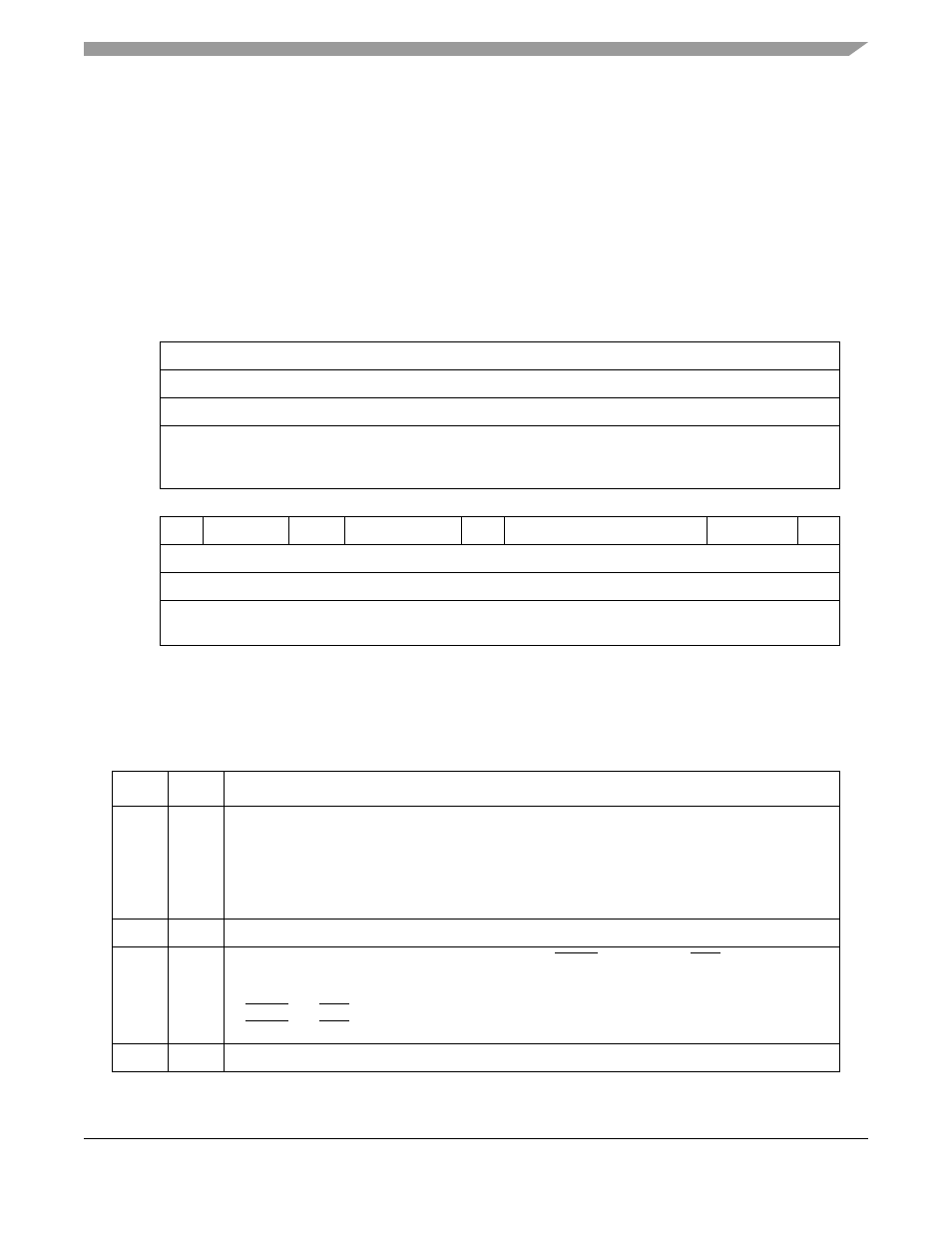
Figure 11-9. OR
x—UPM Mode
Table 11-7. Option Register (OR
x)—UPM Mode
Bits
Name Description
0–16
AM
Address mask. Provides masking for corresponding BR
x
bits. By masking address bits
independently, external devices of different size address ranges can be used. Any clear bit masks
the corresponding address bit. Any set bit causes the corresponding address bit to be used in the
comparison with the address pins. Address mask bits can be set or cleared in any order in the field,
allowing a resource to reside in more than one area of the address map. AM can be read or written
at any time.
17–18
—
Reserved, should be cleared.
19
BCTLD Data buffer control disable. Disables the assertion of BCTL
x
(60x bus) and LWR (local bus) during
an access to the current memory bank. See
Section 11.2.7, “Data Buffer Controls (BCTLx and
.”
0 BCTL
x
and LWR are asserted upon an access to the current memory bank.
1 BCTL
x
and LWR are not asserted upon an access to the current memory bank.
20–22
—
Reserved, should be cleared.