9 sdram mode-set command timing, Figure 11-37. sdram mode-set command timing, Figure 11-38. mode data bit settings – Freescale Semiconductor MPC8260 User Manual
Page 465: 10 sdram refresh, Sdram mode-set command timing -47, Sdram refresh -47, Mode data bit settings -47, Section 11.4.10, “sdram refresh, 9 sdram m, Command timing
Memory Controller
MPC8260 PowerQUICC II Family Reference Manual, Rev. 2
Freescale Semiconductor
11-47
11.4.9
SDRAM M
ODE
-S
ET
Command Timing
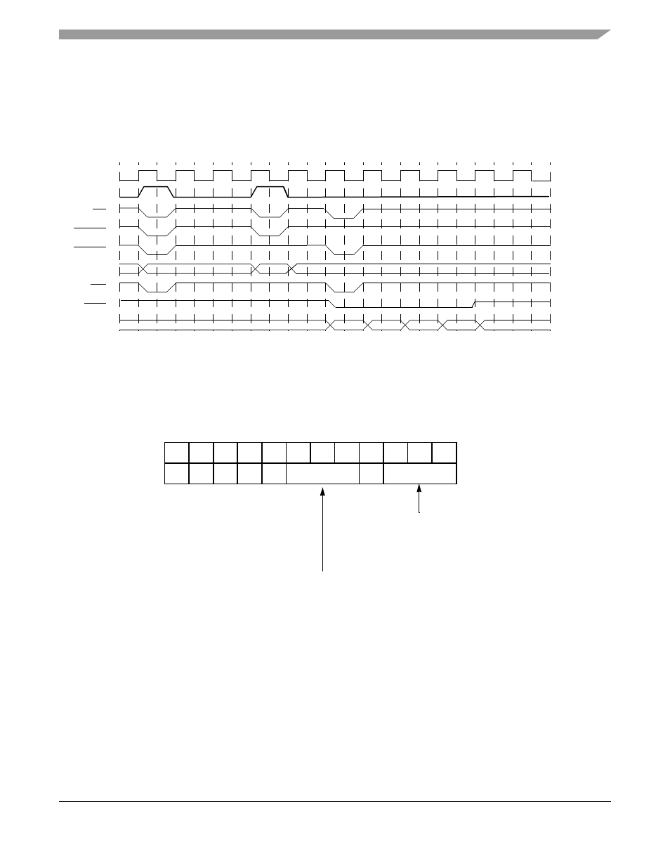
The PowerQUICC II transfers mode register data (CAS latency, burst length, burst type) stored in
P/LSDMR to the SDRAM array by issuing the
MODE
-
SET
command.
shows timing for the
MODE
-
SET
command.
Figure 11-37. SDRAM M
ODE
-S
ET
Command Timing
shows mode data bit settings.
Figure 11-38. Mode Data Bit Settings
11.4.10 SDRAM Refresh
The memory controller supplies auto (CBR) refreshes to SDRAM according to the interval specified in
PSRT or LSRT. This represents the time period required between refreshes. The value of P/LSRT depends
on the specific SDRAM devices used and the operating frequency of the PowerQUICC II’s bus. This value
should allow for a potential collision between memory accesses and refresh cycles. The period of the
refresh interval must be greater than the access time to ensure that read and write operations complete
successfully.
CLK
ALE
CS
SDRAS
SDCAS
MA[0–11]
WE
DQM
Data
Z
Z
D0
D1
D2
D3
*Mode Data
Row
Column
*The mode data is the address value during a mode-set cycle. It is driven by the memory controller, in single
PowerQUICC II mode, according to P/LSDMR[CL] register. In 60x-compatible mode, software must drive the
correct value on the address lines. Figure 11-38. shows the actual value.
Mode Set
Page Activate
Write (Burst)
latency mode—can be 1(001), 2(010), or 3(011).
burst length:
4(010) for 16- and 64-bit port sizes
8(011) for 8- and 32-bit port sizes
Bit number
0
1
2
3
4
5
6
7
8
9
10
11
lsb
CL
0
BL