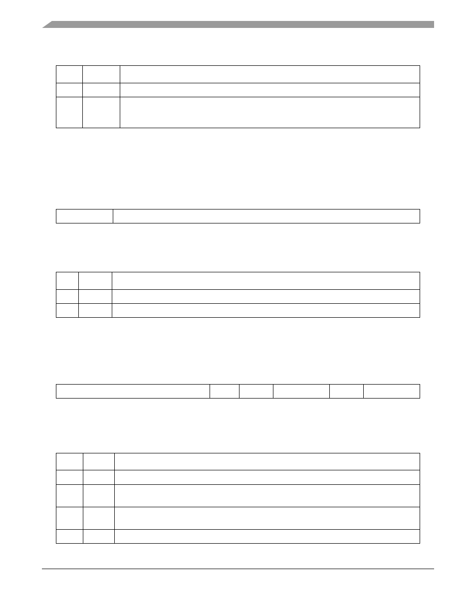
Table 2-2. hid1 field descriptions, Table 2-3. hid2 field descriptions (continued), Hid1 field descriptions -14 – Freescale Semiconductor MPC8260 User Manual
Page 132: Hid2 field descriptions -14
G2 Core
MPC8260 PowerQUICC II Family Reference Manual, Rev. 2
2-14
Freescale Semiconductor
2.3.1.2.2
Hardware Implementation-Dependent Register 1 (HID1)
The PowerQUICC II implementation of HID1 is shown in
.
shows the bit definitions for HID1.
2.3.1.2.3
Hardware Implementation-Dependent Register 2 (HID2)
The processor core implements an additional hardware implementation-dependent register, shown in
describes the HID2 fields.
29–30
—
Reserved
31
NOOPTI
No-op the data cache touch instructions.
0 The dcbt and dcbtst instructions are enabled.
1 The dcbt and dcbtst instructions are no-oped globally.
1
See Chapter 10, “Power Management,” of the
G2 Core Reference Manual
for more information.
2
See Chapter 4, “Instruction and Data Cache Operation,” of the
G2 Core Reference Manual
for more information.
0
4
5
31
PLLCFG
—
Figure 2-4. Hardware Implementation-Dependent Register 1 (HID1)
Table 2-2. HID1 Field Descriptions
Bits
Name
Function
0–4
PLLCFG PLL configuration setting. These bits reflect the state of the PLL_CFG[0:4] signals.
5–31
—
Reserved
0
14
15
16
18 19
23 24
26 27
31
—
SFP
IWLCK
—
DWLCK
—
Figure 2-5. Hardware Implementation-Dependent Register 2 (HID2)
Table 2-3. HID2 Field Descriptions
Bits
Name
Function
0–14
—
Reserved
15
SFP
Speed for low power. Setting SFP reduces power consumption at the cost of reducing the maximum
frequency, which benefits power-sensitive applications that are not frequency-critical.
16–18
IWLCK
Instruction cache way lock. Useful for locking blocks of instructions into the instruction cache for
time-critical applications that require deterministic behavior. See
Section 2.4.2.3, “Cache Locking.”
19–23
—
Reserved
Table 2-1. HID0 Field Descriptions (continued)
Bits
Name
Description