2 mcf548x block diagram, Mcf548x block diagram -2, 2 mcf548 x block diagram – Freescale Semiconductor MCF5480 User Manual
Page 60
MCF548x Reference Manual, Rev. 3
1-2
Freescale Semiconductor
With on-chip support for multiple common communications interfaces, MCF548x products require only
the addition of memories and certain physical layer transceivers to be cost-effective system solutions for
many applications. Such applications include industrial routers, high-end POS terminals, building
automation systems, and process control equipment.
MCF548x products require four supply voltages: 1.5V for the high-performance, low power, internal core
logic, 2.5V for the DDR SDRAM bus interface, 1.25V for the DDR SDRAM V
REF
, and 3.3V for all other
I/O functionality, including the PCI and FlexBus interfaces.
1.2
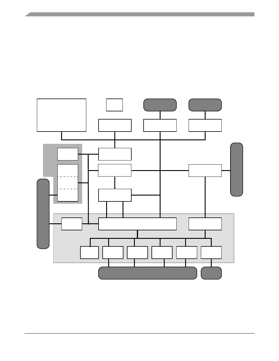
MCF548x Block Diagram
shows a top-level block diagram of the MCF548x products.
1
Available in MCF5485, MCF5484, MCF5483, and MCF5482 devices.
2
Available in MCF5485, MCF5484, MCF5481, and MCF5480 devices.
3
Available in MCF5485, MCF5483, and MCF5481 devices.
Figure 1-1. MCF548x Block Diagram
PLL
DDR SDRAM
Memory
Controller
PCI I/O
Interf
ace and
Ports
CommBus
USB 2.0
PHY
1
Perpheral Communications I/O Interface & Ports
FEC2
2
PSC x 4
I
2
C
FEC1
USB 2.0
DEVICE
1
Interface
FlexBus
Controller
FlexBus
Interface
PCI Interface
& FIFOs
Master/Slave
Interface
ColdFire V4e Core
FPU, MMU
EMAC
32K D-cache
32K I-cache
FlexCAN
x 2
Slave
Bus
DSPI
Pe
rphera
l I/O
Interfa
ce &
Ports
Communicati
ons
I/O S
ubs
ys
te
m
Interrupt
Controller
XL Bus
Arbiter
Sy
st
em
In
tegr
at
io
n
U
ni
t
DM
A
Rea
d
DMA
Wr
ite
Multichannel DMA
Master Bus Interface and FIFOs
Slice
Timers x 2
GP
Timers x 4
Watchdog
Timer
PCI 2.2
Controller
Cryptography
32K System
SRAM
Cr
yp
to
R/W
XL Bus
Read/Write
XL Bus
Accelerator
3