Freescale Semiconductor MCF5480 User Manual
Page 413
Memory Map/Register Definition
MCF548x Reference Manual, Rev. 3
Freescale Semiconductor
16-5
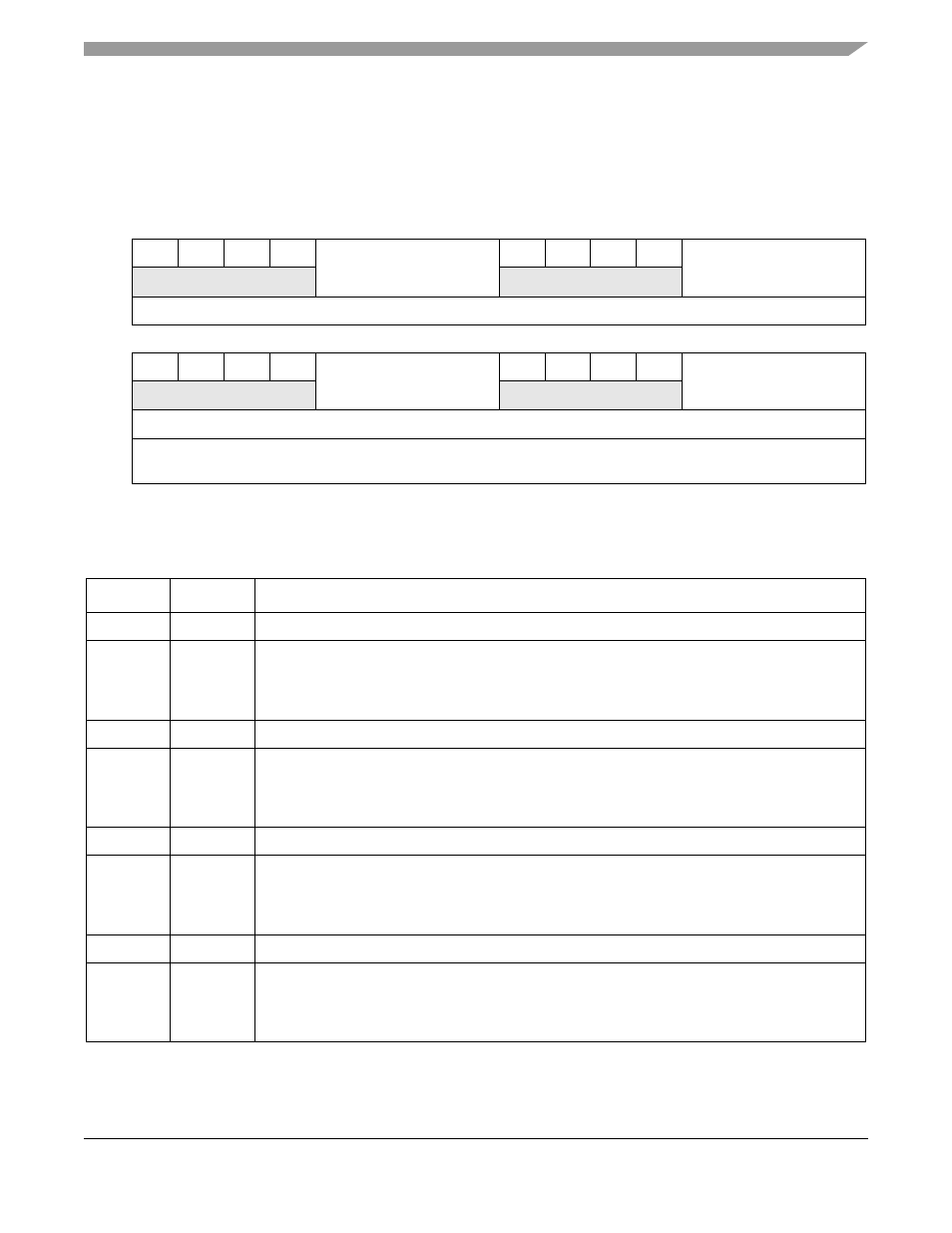
16.2.3
Transfer Count Configuration Register—DMA Read Channel
(TCCRDR)
This register is used to configure the allocated maximum transfer count for each bank for the DMA read
channel as it accesses SRAM directly, without going through the system bus.
Each field is described in the table below.
31
30
29
28
27
26
25
24
23
22
21
20
19
18
17
16
R
0
0
0
0
BANK3_TC
0
0
0
0
BANK2_TC
W
Reset
0
0
0
0
1
1
1
1
0
0
0
0
1
1
1
1
15
14
13
12
11
10
9
8
7
6
5
4
3
2
1
0
R
0
0
0
0
BANK1_TC
0
0
0
0
BANK0_TC
W
Reset
0
0
0
0
1
1
1
1
0
0
0
0
1
1
1
1
Reg
Addr
MBAR + 0x1_FFC8
Figure 16-4. Transfer Count Configuration Register—DMA Read Channel (TCCRDR)
Table 16-4. TCCRDR Register Field Descriptions
Bits
Name Description
31–28
—
Reserved, should be cleared.
27–24
BANK3_TC Bank three transfer count. This field indicates the maximum transfer count for bank 3. The DMA
read channel can make at most 4 * {field value} 32-bit transfers from bank 3 before it must wait for
other masters to complete their transfers. If this field is programmed to “0” the DMA read channel
can “own” bank 3 for arbitrarily long transfers.
23–20
—
Reserved, should be cleared.
19–16
BANK2_TC Bank two transfer count. This field indicates the maximum transfer count for bank 2. The DMA read
channel can make at most 4 * {field value} 32-bit transfers from bank 2 before it must wait for other
masters to complete their transfers. If this field is programmed to “0” the DMA read channel can
“own” bank 2 for arbitrarily long transfers.
15–12
—
Reserved, should be cleared.
11–8
BANK1_TC Bank one transfer count. This field indicates the maximum transfer count for bank 1. The DMA read
channel can make at most 4 * {field value} 32-bit transfers from bank 1 before it must wait for other
masters to complete their transfers. If this field is programmed to “0” the DMA read channel can
“own” bank 1 for arbitrarily long transfers.
7–4
—
Reserved, should be cleared.
3–0
BANK0_TC Bank zero transfer count. This field indicates the maximum transfer count for bank 0. The DMA read
channel can make at most 4 * {field value} 32-bit transfers from bank 0 before it must wait for other
masters to complete their transfers. If this field is programmed to “0” the DMA read channel can
“own” bank 0 for arbitrarily long transfers.