1 7-bit pclrr_x register, 2 5-bit pclrr_x registers, Figure 15-17 – Freescale Semiconductor MCF5480 User Manual
Page 391: The remaining, Their bit definitions are shown in, Figure 15-18
Memory Map/Register Definition
MCF548x Reference Manual, Rev. 3
Freescale Semiconductor
15-19
15.3.2.4.1
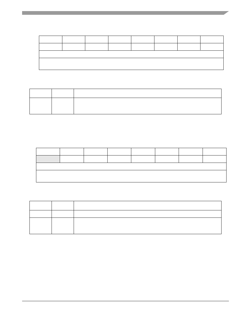
7-Bit PCLRR_x Register
The 7-bit PCLRR_DSPI register is the clear output data register for PDSPIn.
displays the
7-bit PCLRR_DSPI register.
15.3.2.4.2
5-Bit PCLRR_x Registers
The 5-bit PCLRR_x registers are the pin data and set data registers for PPCIBGn (PCLRR_PCIBG) and
PPCIBRn (PCLRR_PCIBR).
displays the 5-bit PCLRR_x registers.
7
6
5
4
3
2
1
0
R
0
0
0
0
0
0
0
0
W
CLRx7
CLRx6
CLRx5
CLRx4
CLRx3
CLRx2
CLRx1
CLRx0
Reset
0
0
0
0
0
0
0
0
Reg
Addr
MBAR + 0xA30 (PCLRR_FBCTL), 0xA34 (PCLRR_FEC0H), 0xA35 (PCLRR_FEC0L), 0xA36 (PCLRR_FEC1H),
0xA37 (PCLRR_FEC1L), 0xA3C (PCLRR_PSC3PSC2), 0xA3D (PCLRR_PSC1PSC0)
Figure 15-17. 8-Bit Port Clear Output Data Registers
Table 15-19. 8-Bit PCLRR_x Field Descriptions
Bits
Name Description
7–0
CLRxn
Clear output data registers
0 Corresponding PODR_x bit is cleared
1 No effect
7
6
5
4
3
2
1
0
R
0
0
0
0
0
0
0
0
W
CLRDSP6
CLRDSP5
CLRDSP4
CLRDSP3
CLRDSP2
CLRDSP1
CLRDSP0
Reset
0
0
0
0
0
0
0
0
Reg
Addr
MBAR + 0xA3E (PCLRR_DSPI)
Figure 15-18. 7-Bit Port Clear Output Data DSPI Register
Table 15-20. 7-Bit PCLRR_DSPI Field Descriptions
Bits
Name Description
7
—
Reserved, should be cleared
6–0
CLRDSPn
PCLRR_DSPI Clear output data register
0 Corresponding PODR_DSPI bit is cleared
1 No effect