Freescale Semiconductor MCF5480 User Manual
Page 946
MCF548x Reference Manual, Rev. 3
30-16
Freescale Semiconductor
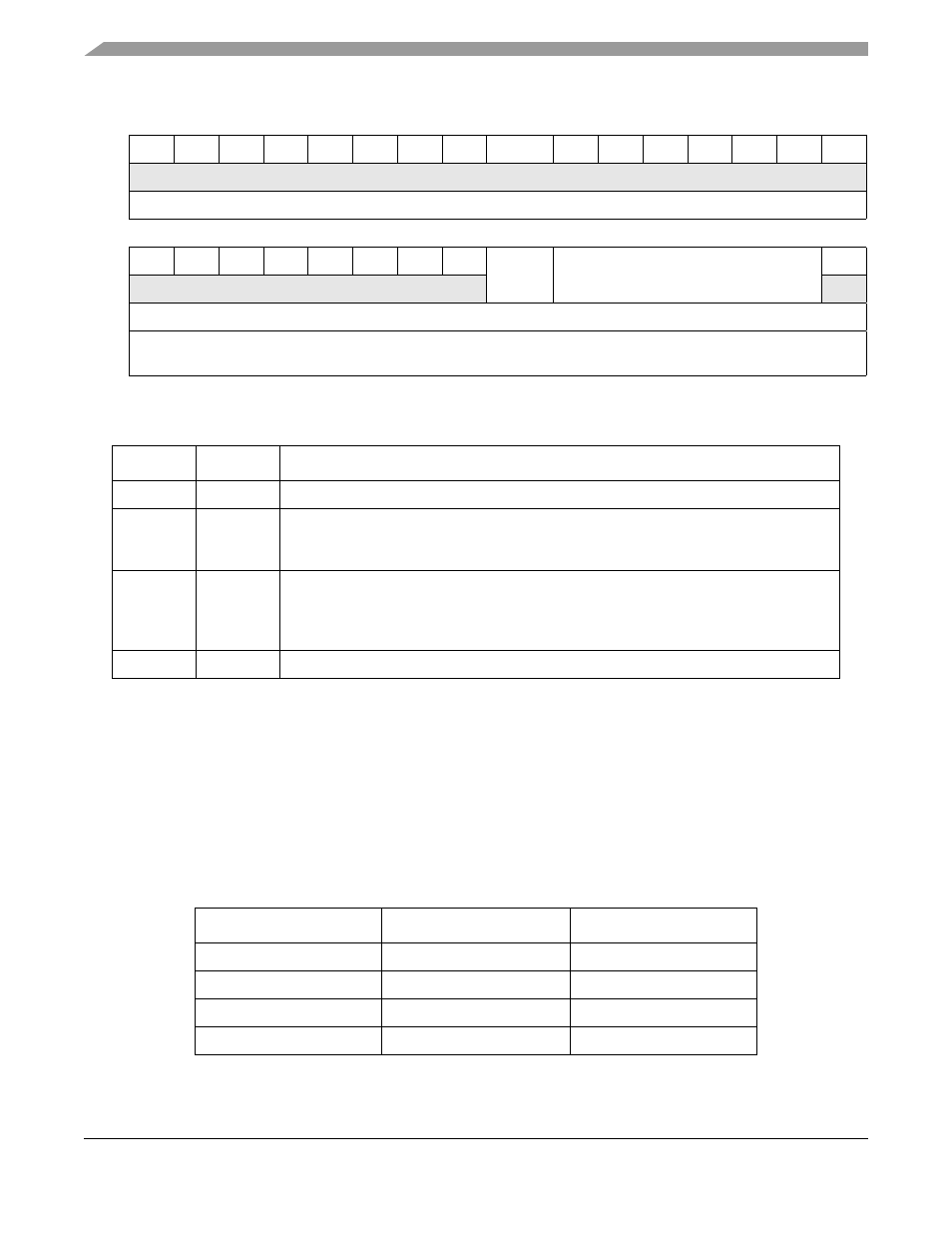
The MII_SPEED field must be programmed with a value to provide an EMDC frequency of less than or
equal to 2.5 MHz to be compliant with the IEEE 802.3 MII specification. The MII_SPEED must be set to
a non-zero value in order to source a read or write management frame. After the management frame is
complete the MSCR register may optionally be set to zero to turn off the EMDC. The EMDC generated
will have a 50% duty cycle except when MII_SPEED is changed during operation (change will take effect
following either a rising or falling edge of EMDC).
If the system clock is 66 MHz, programming the MII_SPEED field to 0x5 will result in an EMDC
frequency of 66 MHz
× 1/26 = 2.5 MHz. A table showing optimum values for MII_SPEED as a function
of system clock frequency is provided below.
31
30
29
28
27
26
25
24
23
22
21
20
19
18
17
16
R
0
0
0
0
0
0
0
0
0
0
0
0
0
0
0
0
W
Reset
0
0
0
0
0
0
0
0
0
0
0
0
0
0
0
0
15
14
13
12
11
10
9
8
7
6
5
4
3
2
1
0
R
0
0
0
0
0
0
0
0
DIS_PRE
AMBLE
MII_SPEED
0
W
Reset
0
0
0
0
0
0
0
0
0
0
0
0
0
0
0
0
Reg
Addr
MBAR + 0x9044 (FEC0), 0x9844 (FEC1)
Figure 30-6. MII Speed Control Register (MSCR)
Table 30-11. MSCR Field Descriptions
Bits
Name
Description
31–8
—
Reserved, should be cleared.
7
DIS_PRE
AMBLE
Asserting this bit will cause preamble (32 1’s) not to be prepended to the MII management
frame. The MII standard allows the preamble to be dropped if the attached PHY devices
do not require it.
6–1
MII_SPEED MII_SPEED controls the frequency of the MII management interface clock (EMDC) relative
to the system clock (which for the FEC module is the IP bus). A value of 0 in this field will
“turn off” the EMDC and leave it in low voltage state. Any non-zero value will result in the
EMDC frequency of 1/(MII_SPEED*2) of the system clock frequency.
0
—
Reserved, should be cleared.
Table 30-12. Programming Examples for MSCR
Clock Frequency
MII_SPEED (field in reg)
EMDC frequency
60 MHz
0xC
2.5 MHz
66 MHz
0xD
2.5 MHz
120 MHz
0x18
2.5 MHz
133 MHz
0x1A
2.5 MHz