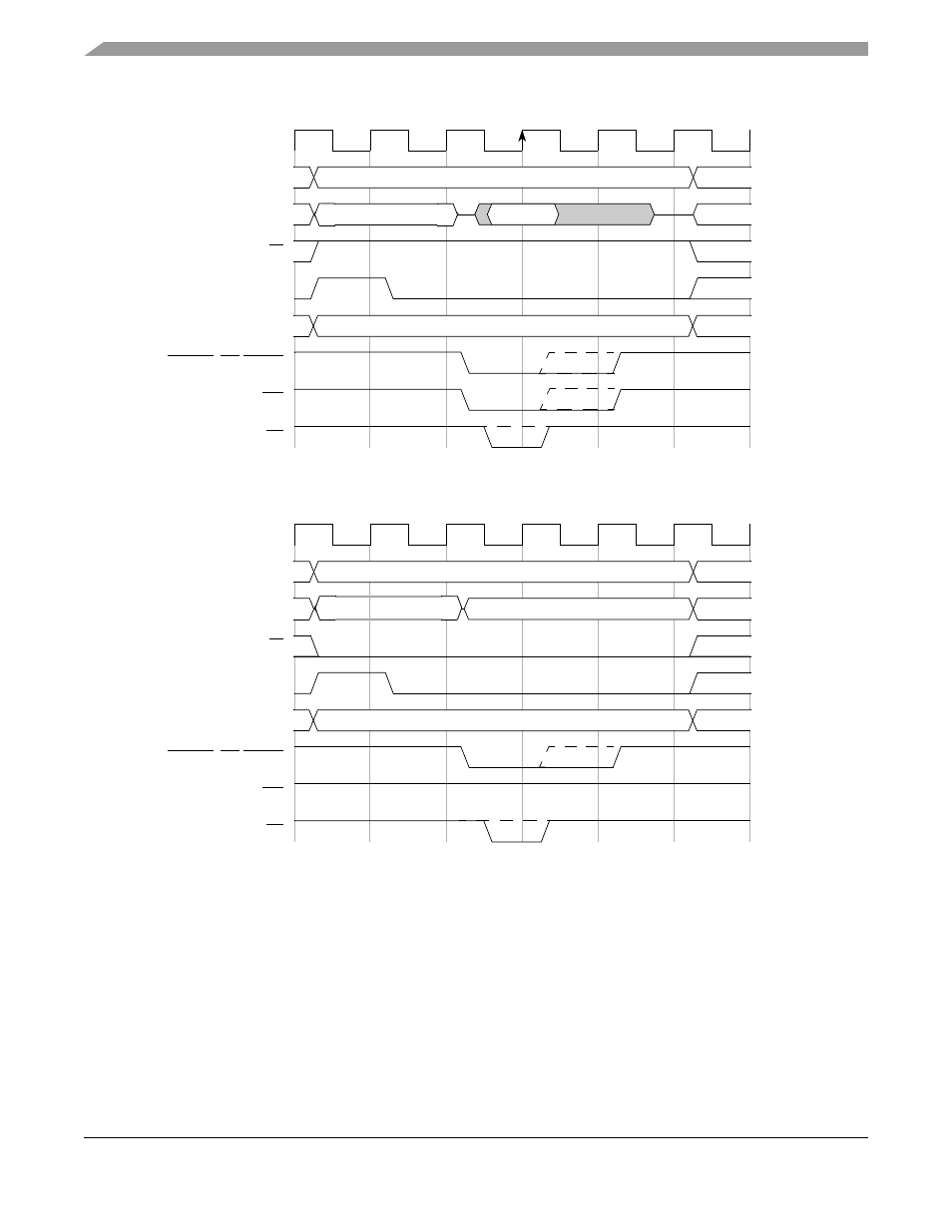
Latch enable (ale) is asserted, Figure 17-22, Figure 17-23 – Freescale Semiconductor MCF5480 User Manual
Page 440: Show read and wr
MCF548x Reference Manual, Rev. 3
17-24
Freescale Semiconductor
Figure 17-22. Read Bus Cycle with Two Clock Address Setup (No Wait States)
Figure 17-23. Write Bus Cycle with Two Clock Address Setup (No Wait States)
In addition to address setup, there is also a programmable address hold option for each chip select. Address
and attributes can be held one to four clocks after chip select, byte selects, and output enable negate.
and
show read and write bus cycles with two clocks of address hold.
CLK
AD[X:0]
AD[31:Y]
R/W
ALE
TA
OE
S0
AS
S1
S2
S3
FBCSn, BE/BWEn
ADDR[X:0]
A[31:Y]
TSIZ[1:0]
TSIZ[1:0]
DATA
CLK
AD[X:0]
AD[31:Y]
R/W
ALE
TA
OE
S0
AS
S1
S2
S3
FBCSn, BE/BWEn
ADDR[X:0]
DATA
TSIZ[1:0]
TSIZ[1:0]
A[31:Y]