9 perform two refresh cycles, Perform two refresh cycles -31 – Freescale Semiconductor MCF5480 User Manual
Page 479
SDRAM Example
MCF548x Reference Manual, Rev. 3
Freescale Semiconductor
18-31
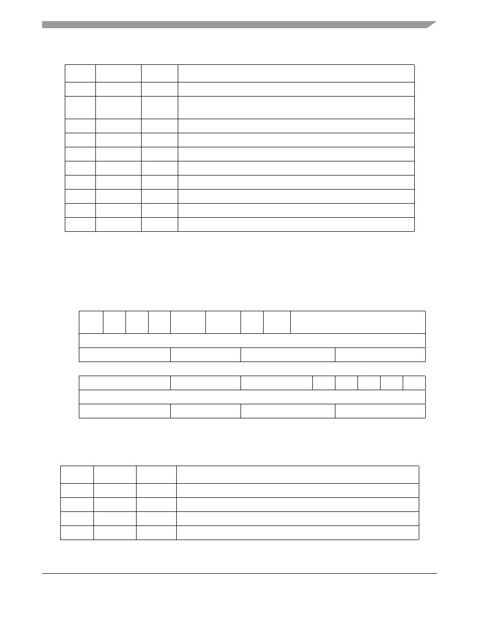
18.8.9
Perform Two Refresh Cycles
The SDCR should be programmed as shown in
. Along with the base settings for the SDCR
the MODE_EN and IREF bits are set to issue an REF command to the SDRAM and enable writing of the
mode register. The memory used in this example requires two refresh cycles, so this step is repeated twice.
This configuration results in a value of SDCR = 0xE10D_0004, as described in
Table 18-19
.
22
DRIVE
0
Data and DQS lines are only driven for a write cycle.
21–16
RCNT
001101
RCNT = (t
REFI
/ (SDCLK x 64)) - 1 = (7800ns/(8.3ns x 64)) - 1 = 13.62,
round down to 13 (0xD)
15–12
—
0000
Reserved. Should be cleared.
11–8
DQS_OE
0000
0x0 disables drive for all SDDQS pins for now.
7–5
—
000
Reserved. Should be cleared.
4
BUFF
0
0 indicates that a buffered memory module is not being used.
3
—
0
Reserved. Should be cleared.
2
IREF
0
Do not initiate a REF command.
1
IPALL
1
Initiate a PALL command.
0
—
0
Reserved. Should be cleared.
31
30
29
28
27
26
25
24
23
22
21
20
19
18
17
16
Field MODE
_EN
CKE
DDR
REF
—
MUX
AP
DRIVE
RCNT
Setting
1110_0001_0000_1101
(hex)
E
1
0
D
15
14
13
12
11
10
9
8
7
6
5
4
3
2
1
0
Field
—
DQS_OE
—
BUFF
—
IREF IPALL
—
Setting
0000_0000_0000_0100
(hex)
0
0
0
4
Figure 18-22. SDRAM Control Register Settings + MODE_EN and IREF
Table 18-23. SDCR + MODE_EN and IREF Field Descriptions
Bits
Name
Setting
Description
31
MODE_EN
1
Mode register is writable.
30
CKE
1
SDCKE is asserted
29
DDR
1
DDR mode is enabled
28
REF
0
Automatic refresh is disabled
Table 18-22. SDCR + MODE_EN and IPALL Field Descriptions (Continued)
Bits
Name
Setting
Description