5 base address register 0 (pcibar0)-pci dword 4, Base address register 0 (pcibar0)—pci dword 4 -11, 5 base address register 0 (pcibar0)—pci dword 4 – Freescale Semiconductor MCF5480 User Manual
Page 495
Memory Map/Register Definition
MCF548x Reference Manual, Rev. 3
Freescale Semiconductor
19-11
19.3.1.5
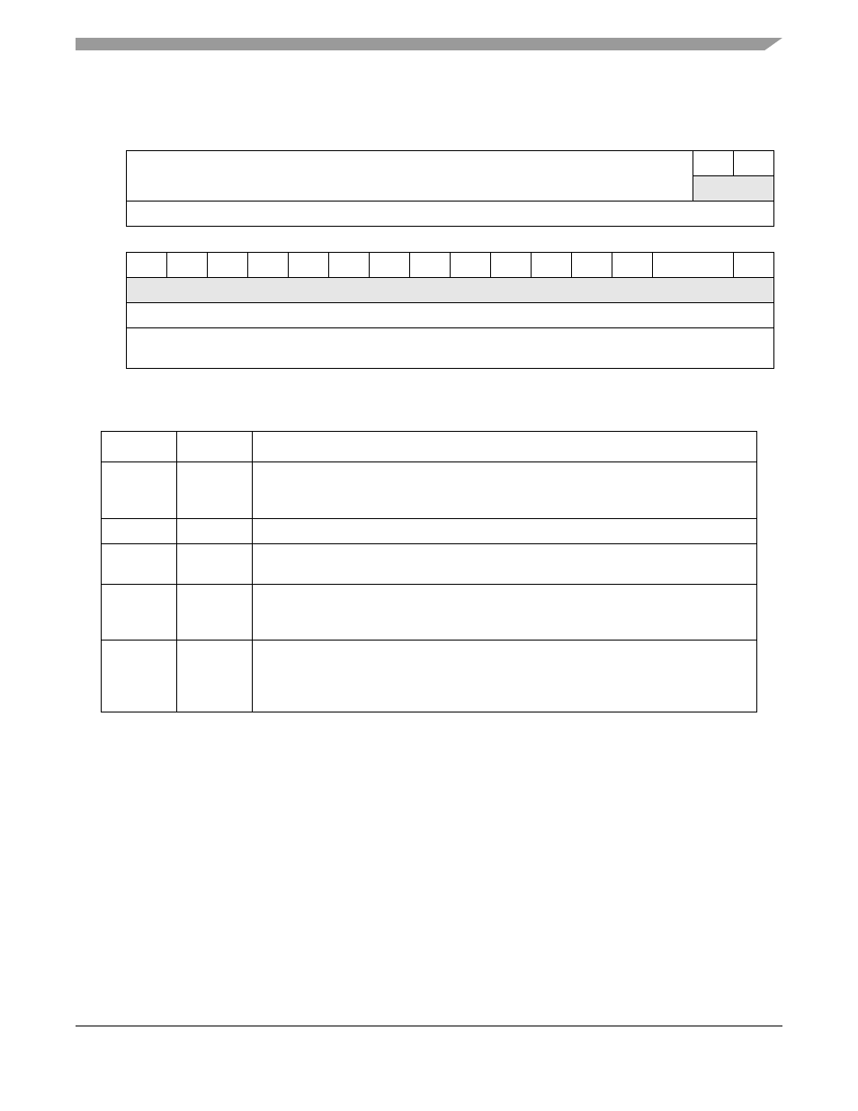
Base Address Register 0 (PCIBAR0)—PCI Dword 4
31
30
29
28
27
26
25
24
23
22
21
20
19
18
17
16
R
BAR 0
0
0
W
Reset
0
0
0
0
0
0
0
0
0
0
0
0
0
0
0
0
15
14
13
12
11
10
9
8
7
6
5
4
3
2
1
0
R
0
0
0
0
0
0
0
0
0
0
0
0
PREF
RANGE
IO/M#
W
Reset
0
0
0
0
0
0
0
0
0
0
0
0
0
0
0
0
Reg
Addr
MBAR + 0xB10
Figure 19-6. Base Address Register 0 (PCIBAR0)
Table 19-7. PCIBAR0 Field Descriptions
Bits
Name
Description
31–18
BAR0
Base address register 0. PCI base address register 0 (256 Kbyte). Applies only when
processor is target. These bits are programmable (read/write from both the IP bus and PCI
bus Configuration cycles).
17–4
—
Reserved, should be cleared.
3
PREF
Prefetchable access. Fixed to 0. This bit indicates that the memory space defined by BAR0
is not prefetchable. Configuration software should write a 0 to this bit location.
2–1
RANGE
Fixed to 00. This register indicates that base address 0 is 32 bits wide and can be mapped
anywhere in 32-bit address space. Configuration software should write 00 to these bit
locations.
0
IO/M#
IO or memory space. Fixed to 0. This bit indicates that BAR0 is for memory space.
Configuration software should write a 0 to this bit location.
0 Memory
1 I/O