3 communication subsystem interface registers, 1 comm bus fifo transmit interface, 1 tx packet size register (pcitpsr) – Freescale Semiconductor MCF5480 User Manual
Page 507: Communication subsystem interface registers -23, Comm bus fifo transmit interface -23
Memory Map/Register Definition
MCF548x Reference Manual, Rev. 3
Freescale Semiconductor
19-23
19.3.3
Communication Subsystem Interface Registers
The communication subsystem/multichannel DMA interface has separate control registers for transmit
and receive operations.
19.3.3.1
Comm Bus FIFO Transmit Interface
PCI Tx is controlled by 14 32-bit registers. These registers are located at an offset from MBAR of 0x8400.
Register addresses are relative to this offset.
19.3.3.1.1
Tx Packet Size Register (PCITPSR)
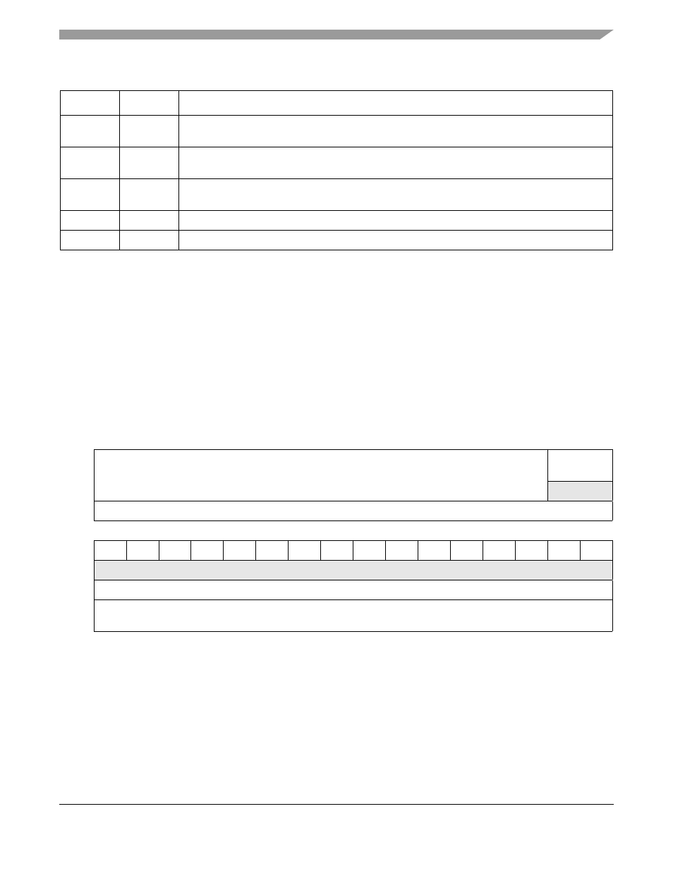
23–16
Bus
Number
This register field is an encoded value used to select the target bus of the configuration access. For
target devices on the PCI bus connected to MCF548, this field should be set to 0x00.
15–11
Device
Number
This field is used to select a specific device on the target bus.
Section 19.4.4.2, “Configuration
for more information.
10–8
Function
Number
This field is used to select a specific function in the requested device. Single-function devices
should respond to function number ‘000’.
7–2
DWORD
This field is used to select the Dword address offset in the configuration space of the target device.
1–0
—
Reserved, should be cleared.
31
30
29
28
27
26
25
24
23
22
21
20
19
18
17
16
R
Packet_Size[15:2]
Packet_Size
[1:0]
W
Reset
0
0
0
0
0
0
0
0
0
0
0
0
0
0
0
0
15
14
13
12
11
10
9
8
7
6
5
4
3
2
1
0
R
0
0
0
0
0
0
0
0
0
0
0
0
0
0
0
0
W
Reset
0
0
0
0
0
0
0
0
0
0
0
0
0
0
0
0
Reg
Addr
MBAR + 0x8400
Figure 19-20. Tx Packet Size Register (PCITPSR)
Table 19-18.
PCICAR Field Descriptions (Continued)
Bits
Name
Description