Section 27.7.4.4, Modified spi transfer format (mtfe = 1, cpha = 1), Figure 27-17 – Freescale Semiconductor MCF5480 User Manual
Page 846: 1, cpha = 1)
MCF548x Reference Manual, Rev. 3
27-28
Freescale Semiconductor
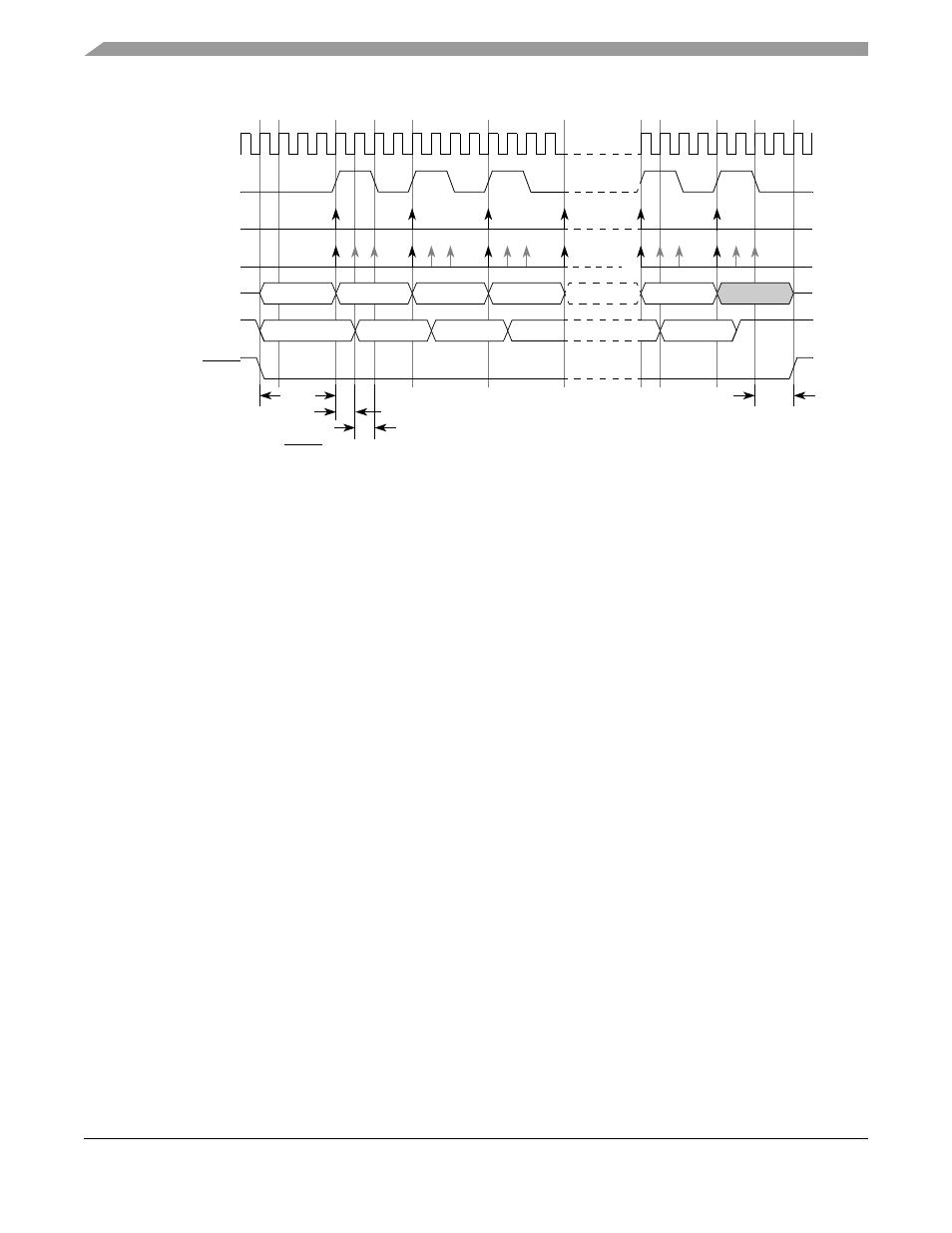
Figure 27-17. DSPI Modified Transfer Format (MTFE = 1, CPHA = 0, Fsck = Fsys/4)
27.7.4.4
Modified SPI Transfer Format (MTFE = 1, CPHA = 1)
shows the modified transfer format for CPHA = 1. Only the condition where CPOL = 0 is
described. At the start of a transfer the DSPI asserts the CSn signal to the slave device. After the CS to
DSPISCK delay has elapsed, the master and the slave put data on their DSPISOUT pins at the first edge
of DSPISCK. The slave samples the master DSPISOUT signal on the even numbered edges of DSPISCK.
The master samples the slave DSPISOUT signal on the odd numbered DSPISCK edges, starting with the
third DSPISCK edge. The slave samples the last bit on the last edge of the DSPISCK. The master samples
the last slave DSPISOUT bit one-half DSPISCK cycle after the last edge of DSPISCK. No clock edge will
t
CSC
= PCSS to DSPISCK delay
t
ASC
= After DSPISCK delay
System Clock
1
2
3
4
5
6
PCSS
t
ASC
DSPISCK
Master Sample
Slave DSPISOUT
Master DSPISOUT
System Clock
System Clock
Slave Sample
t
CSC