14 tx fifo write pointer register (pcitfwpr), 2 comm bus fifo receive interface, Comm bus fifo receive interface -35 – Freescale Semiconductor MCF5480 User Manual
Page 519
Memory Map/Register Definition
MCF548x Reference Manual, Rev. 3
Freescale Semiconductor
19-35
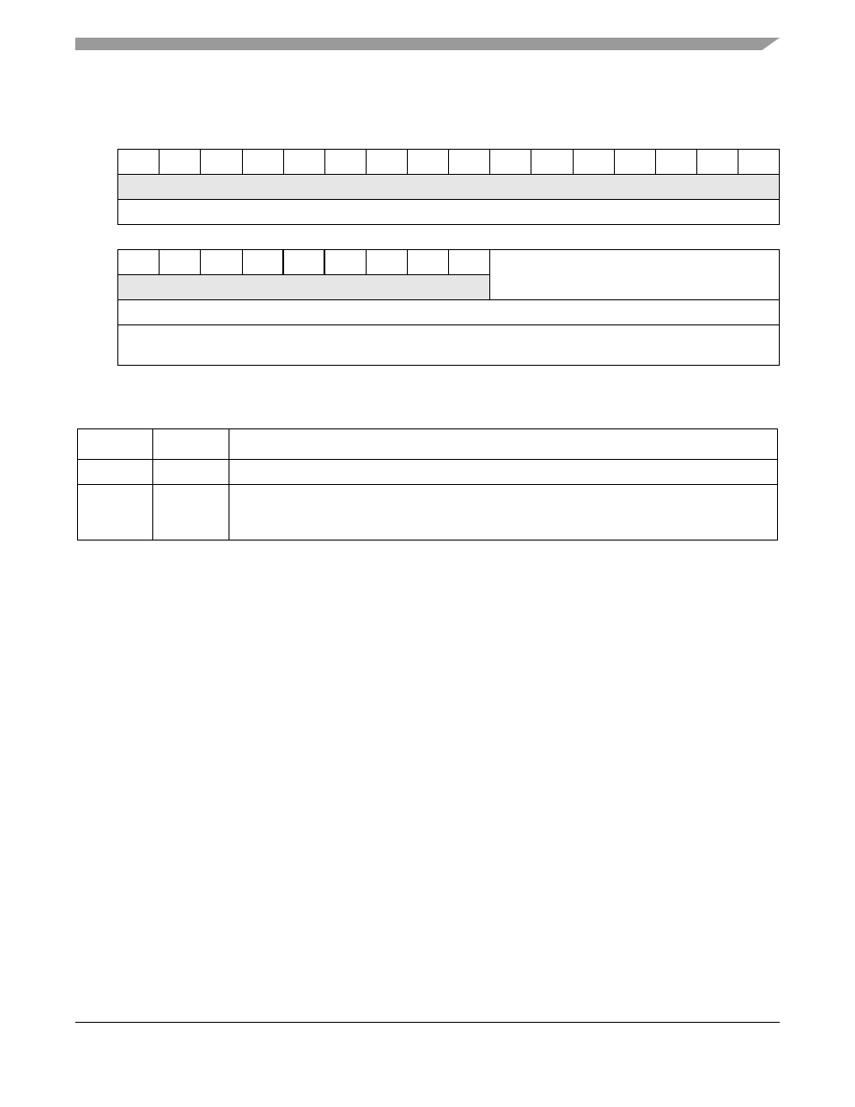
19.3.3.1.14 Tx FIFO Write Pointer Register (PCITFWPR)
This marks the end of the PCI Comm Bus FIFO Transmit Interface description.
19.3.3.2
Comm Bus FIFO Receive Interface
PCI Rx is controlled by 13 32-bit registers. These registers are located at an offset from MBAR. Register
addresses are relative to this offset.
31
30
29
28
27
26
25
24
23
22
21
20
19
18
17
16
R
0
0
0
0
0
0
0
0
0
0
0
0
0
0
0
0
W
Reset
0
0
0
0
0
0
0
0
0
0
0
0
0
0
0
0
15
14
13
12
11
10
9
8
7
6
5
4
3
2
1
0
R
0
0
0
0
0
0
0
0
0
WritePtr
W
Reset
0
0
0
0
0
0
0
0
0
0
0
0
0
0
0
0
Reg
Addr
MBAR + 0x8454
Figure 19-33. Tx FIFO Write Pointer Register (PCITFWPR)
Table 19-32. PCITFWPR Field Descriptions
Bits
Name
Description
31–7
—
Reserved, should be cleared.
6–0
WritePtr
Value is maintained by FIFO hardware and is not normally written by user. It can be adjusted in
special cases, but this disrupts data flow integrity. Value represents the Write address presented
to the FIFO RAM.