Freescale Semiconductor MCF5480 User Manual
Page 735
Memory Map/Register Definitions
MCF548x Reference Manual, Rev. 3
Freescale Semiconductor
24-15
31
30
29
28
27
26
25
24
23
22
21
20
19
18
17
16
TASK0
TASK1
TASK2
TASK3
R
SRCSZ
DSTSZ
SRCSZ
DSTSZ
SRCSZ
DSTSZ
SRCSZ
DSTSZ
W
Reset
0
0
0
0
0
0
0
0
0
0
0
0
0
0
0
0
15
14
13
12
11
10
9
8
7
6
5
4
3
2
1
0
TASK4
TASK5
TASK6
TASK7
R
SRCSZ
DSTSZ
SRCSZ
DSTSZ
SRCSZ
DSTSZ
SRCSZ
DSTSZ
W
Reset
0
0
0
0
0
0
0
0
0
0
0
0
0
0
0
0
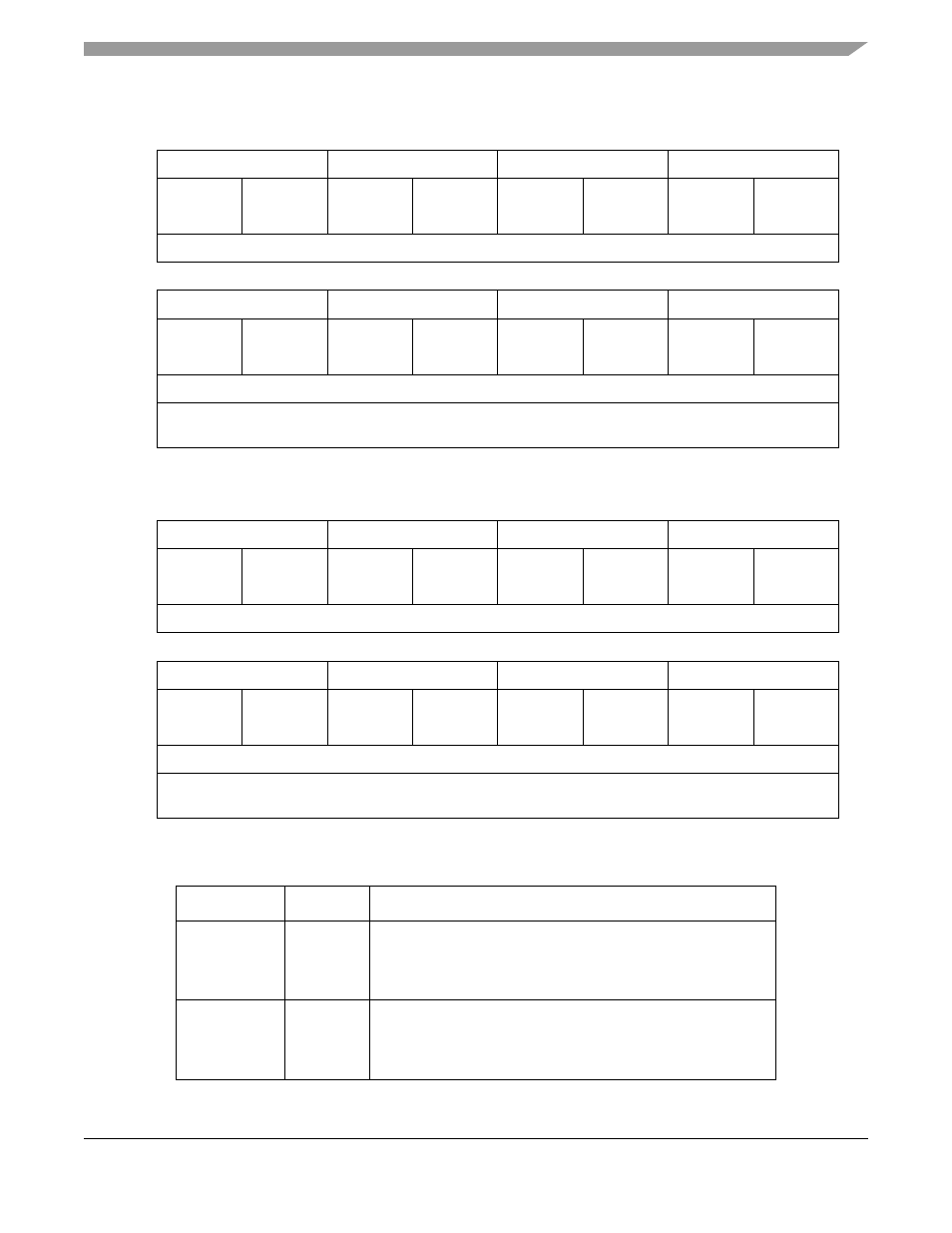
Reg
Addr
MBAR + 0x8060 (TSKSZ0)
Figure 24-14. Task Size Register 0 (TSKSZ0)
31
30
29
28
27
26
25
24
23
22
21
20
19
18
17
16
TASK8
TASK9
TASK10
TASK11
R
SRCSZ
DSTSZ
SRCSZ
DSTSZ
SRCSZ
DSTSZ
SRCSZ
DSTSZ
W
Reset
0
0
0
0
0
0
0
0
0
0
0
0
0
0
0
0
15
14
13
12
11
10
9
8
7
6
5
4
3
2
1
0
TASK12
TASK13
TASK14
TASK15
R
SRCSZ
DSTSZ
SRCSZ
DSTSZ
SRCSZ
DSTSZ
SRCSZ
DSTSZ
W
Reset
0
0
0
0
0
0
0
0
0
0
0
0
0
0
0
0
Reg
Addr
MBAR +0x8064 (TSKSZ1)
Figure 24-15. Task Size Register 1 (TSKSZ1)
Table 24-11. TSKSZ Field Descriptions
Bits
Name
Descriptions
31:30, 27:26,
23:22, 19:18,
15:14, 11:10,
7:6, 3:2
SRCSZ
Source size
00 Longword
01 Byte
1x Word
29:28, 25:24,
21:20, 17:16,
13:12, 9:8, 5:4,
1:0
DSTSZ
Destination size
00 Longword
01 Byte
1x Word