2 mcf548x external signals, 1 flexbus signals, 1 address/data bus (ad[31:0]) – Freescale Semiconductor MCF5480 User Manual
Page 86: Mcf548x external signals -16, Flexbus signals -16, Address/data bus (ad[31:0]) -16, 2 mcf548 x external signals
MCF548x Reference Manual, Rev. 3
2-16
Freescale Semiconductor
2.2
MCF548x External Signals
2.2.1
FlexBus Signals
2.2.1.1
Address/Data Bus (AD[31:0])
The AD[31:0] bus carries address and data. The full 32-bit address is always driven on the first clock of a
bus cycle (address phase). The number of bytes used for data during the data phase is determined by the
port size associated with the matching chip select.
M16
VSS
—
—
—
AF8
1
E1COL
PFEC1H4
—
—
M23
VSS
—
—
—
AF9
E0TXCLK
PFEC0H7
—
—
M24
EVDD
—
—
—
AF10
E0MDIO
PFECI2C3
—
—
M25
PCIAD12
—
FBADDR12
—
AF11
E0RXD3
PFEC0L3
—
—
M26
PCIAD13
—
FBADDR13
—
AF12
E0RXD2
PFEC0L2
—
—
N1
SDCLK0
—
—
—
AF13
E0RXD1
PFEC0L1
—
—
N2
SDCLK0
—
—
—
AF14
3
USBCLKOUT
—
—
—
N3
SDCS0
—
—
—
AF15
USBCLKIN
—
—
—
N4
SDDATA7
—
—
—
AF16
USBD+
—
—
—
N11
VSS
—
—
—
AF17
USBD-
—
—
—
N12
VSS
—
—
—
AF18
USBRBIAS
—
—
—
N13
VSS
—
—
—
AF19
DREQ1
PDMA1
TIN1
IRQ1
N14
VSS
—
—
—
AF20
DREQ0
PDMA0
TIN0
—
N15
VSS
—
—
—
AF21
TIN2
PTIM5
IRQ2
CANRX1
N16
VSS
—
—
—
AF22
TIN0
—
—
—
N23
PCIAD16
—
FBADDR16
—
AF23
PSC3CTS
PPSC3PSC27
PSC3BCLK
—
N24
PCIAD14
—
FBADDR14
—
AF24
1
E1RXD0
PFEC1H1
—
—
N25
PCIAD17
—
FBADDR17
—
AF25
PSC1CTS
PPSC1PSC07
PSC1BCLK
—
N26
PCIAD15
—
FBADDR15
—
AF26
TOUT0
—
—
—
1
This pin is a “no connect” on the MCF5483 and MCF5482 devices.
2
This pin is a “no connect” on the MCF5481 and MCF5480 devices. On MCF5485, MCF5484, MCF5483, and MCF5482 device the pin
should be connected to the appriopriate power rail even is USB is not being used.
3
This pin is a “no connect” on the MCF5481 and MCF5480 devices.
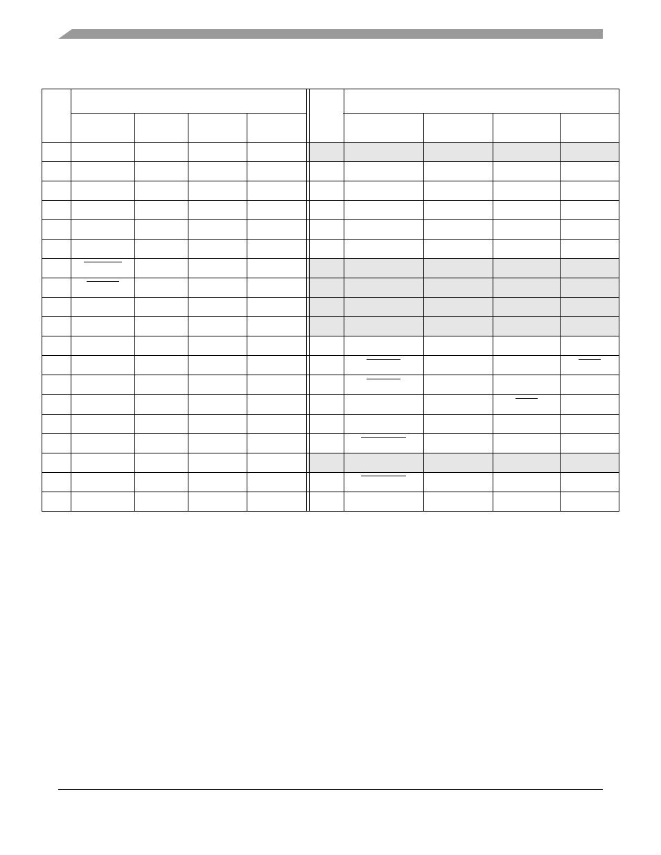
Table 2-2. MCF5485/MCF5484 Signal Description by Pin Number (Continued)
PBGA Pin
Pin Functions
PBGA Pin
Pin Functions
Primary
GPIO
Secondary
Tertiary
Primary
GPIO
Secondary
Tertiary