5 usb endpoint n fifo data register (epnfdr), Usb endpoint, 5 usb endpoint n fifo data register (ep n fdr) – Freescale Semiconductor MCF5480 User Manual
Page 913
Memory Map/Register Definition
MCF548x Reference Manual, Rev. 3
Freescale Semiconductor
29-39
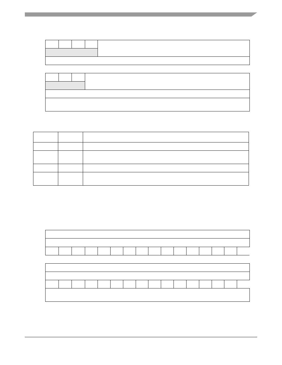
29.2.5.5
USB Endpoint n FIFO Data Register (EPnFDR)
The EPnFDR is the main interface port for the FIFO. Data that is to be buffered in the FIFO, or has been
buffered in the FIFO, is accessed through this register. The register can access data from the FIFO,
independent of this FIFO’s transmit or receive configuration.
31
30
29
28
27
26
25
24
23
22
21
20
19
18
17
16
R
0
0
0
0
BASE
W
Reset
Uninitialized
15
14
13
12
11
10
9
8
7
6
5
4
3
2
1
0
R
0
0
0
DEPTH
W
Reset
Uninitialized
Reg
Addr
MBAR + 0xB44C (EP0FRCFGR); 0xB47C (EP1FRCFGR); 0xB4AC (EP2FRCFGR); 0xB4DC (EP3FRCFGR);
0xB50C (EP4FRCFGR); 0xB53C (EP5FRCFGR); 0xB56C (EP6FRCFGR)
Figure 29-44. USB Endpoint n FIFO RAM Configuration Register (EPnFRCFGR)
Table 29-39. EPnFRCFGR Field Descriptions
Bits
Name
Description
31–28
—
Reserved, should be cleared.
27–16
BASE
Base address. This byte value indicates the base address within the FIFO RAM at which
the allocated space begins.
15–13
—
Reserved, should be cleared.
12–0
DEPTH
Depth. This indicates the depth (in bytes) of the endpoint FIFO. The value should be line
aligned to ensure proper operation (that is, DEPTH[2:0] must be set to 0).
31
30
29
28
27
26
25
24
23
22
21
20
19
18
17
16
R
RXDATA[31:16]
W
TXDATA[31:16]
Reset
U
U
U
U
U
U
U
U
U
U
U
U
U
U
U
U
15
14
13
12
11
10
9
8
7
6
5
4
3
2
1
0
R
RXDATA[15:0]
W
TXDATA[15:0]
Reset
U
U
U
U
U
U
U
U
U
U
U
U
U
U
U
U
Reg
Addr
MBAR + 0xB450 (EP0FDR); 0xB480 (EP1FDR); 0xB4B0 (EP2FDR); 0xB4E0 (EP3FDR);
0xB510 (EP4FDR); 0xB540 (EP5FDR); 0xB570 (EP6FDR)
Figure 29-45. USB Endpoint n FIFO Data Register (EPnFDR)