Freescale Semiconductor MCF5480 User Manual
Page 53
Terminology and Notational Conventions
MCF548x Reference Manual, Rev. 3
Freescale Semiconductor
liii
Bits BA, DT, and AT: The 0 and 1 are switched. Setting each bit enables operation, while clearing disables
operation. The 0 and 1 (or the corresponding descriptions) need to be swapped for all three bits.
Remove all text from bullet item #2 starting with “This scenario works for all pulses except....” This errata
does not apply to this processor.
Correct the cross-reference link at top of page that reads “Section 3.8.1, ‘Exception Stack Frame
Definition.’”
In the bit 7-6, PAR1_E1MDC entry, change ‘11’ bit setting description from: “E1MDC pin configured for
FEC1 MDC function” to “E1MDC pin configured for FEC1 E1MDC function” to be consistent with rest of
section.
Remove extraneous “/” from “DSPICS0//SS” in second sentence of the PAR_CS0 bit description.
Extend SSCR entry to include bytes 2 & 3 as well as bytes 0 and 1, since it is a 32 bit register.
Change “transfer start” to “address latch enable” in second sentence.
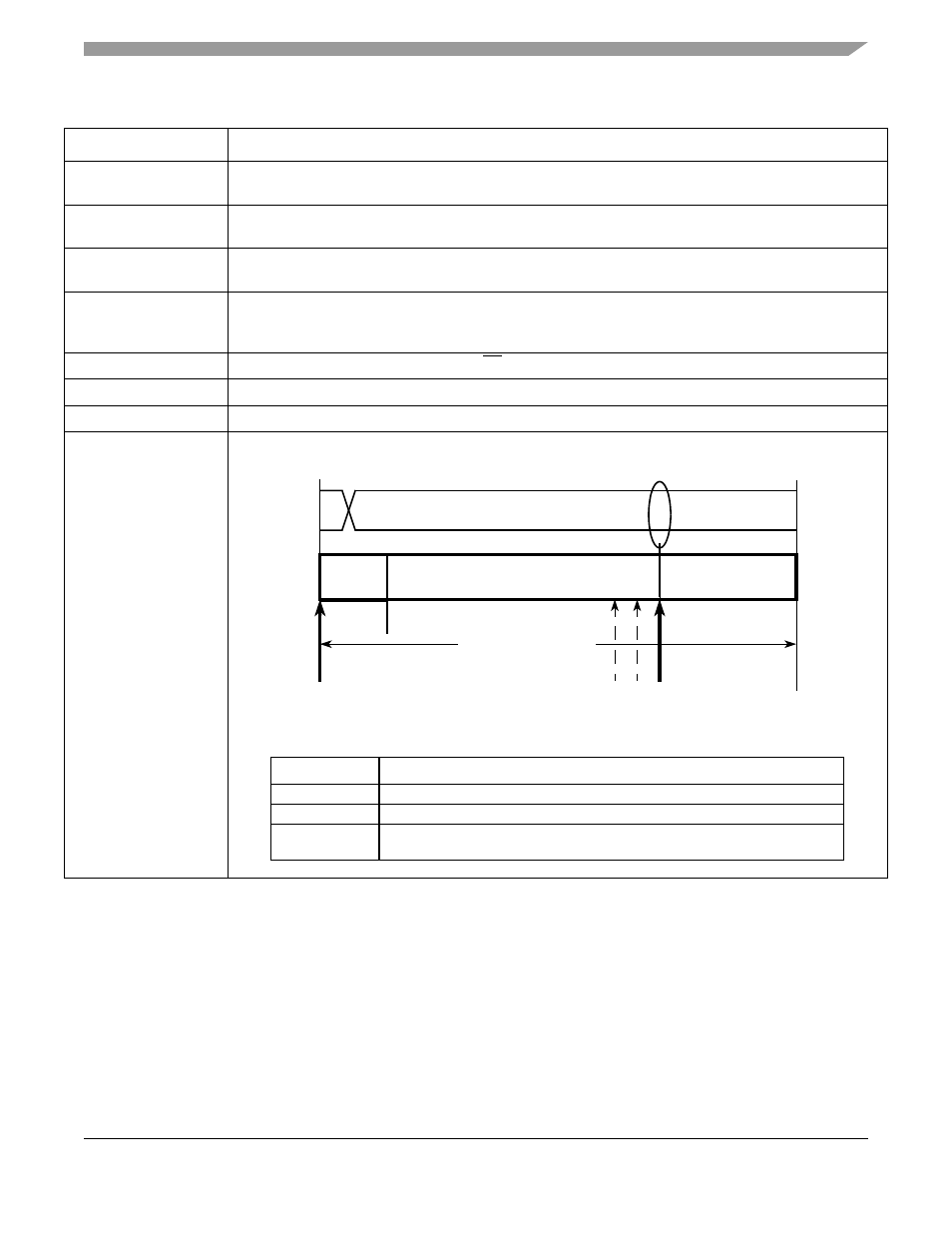
Figure 21-14 and Table 21-18 are missing. Add them as shown below and correct the cross-references to
them.
Table iv. MCF548x Revision History (continued)
Section/Page
Substantive Changes
Figure 21-14. Segments within the Bit Time
Table 21-18. Time Segment Syntax
Syntax
Description
SYNC_SEG
System expects transitions to occur on the bus during this period.
Transmit Point
A node in transmit mode transfers a new value to the CAN bus at this point.
Sample Point
A node samples the bus at this point. If the three samples per bit option is selected,
then this point marks the position of the third sample.
SYNC_SEG
Time Segment 1
Time Segment 2
1
4 ... 16
2 ... 8
8 ... 25 Time Quanta
= 1 Bit Time
NRZ Signal
Sample Point
(single or triple sampling)
(PROP_SEG + PSEG1 + 2)
(PSEG2 + 1)
Transmit Point