2 clocking overview, 3 internal bus overview, Clocking overview -2 – Freescale Semiconductor MCF5480 User Manual
Page 324: Internal bus overview -2
MCF548x Reference Manual, Rev. 3
10-2
Freescale Semiconductor
10.1.2
Clocking Overview
The MCF548x requires a clock generated externally to be input to the CLKIN signal. The MCF548x uses
this clock as the reference clock for the internal PLL. The internal PLL then generates the clocks needed
by the CPU core and integrated peripherals.
The external PCI and FlexBus signals are always clocked at the same frequency as the CLKIN signal. A
programmable clock multiplier (determined by the AD[12:8] signals at reset) is used to determine the XL
bus frequency. All integrated peripherals and the 32KB system SRAM are clocked at the same frequency
as the XLB. The ColdFire V4e core complex (core, MMU, FPU, SRAMs, etc.) is always clocked at twice
the XLB frequency.
shows the supported PLL encodings and the corresponding clock frequency ranges.
correlates CLKIN, internal bus, and core clock frequencies for the 1x–4x multipliers.
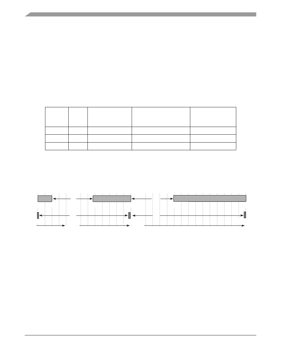
Figure 10-2. CLKIN, Internal Bus, and Core Clock Ratios
10.1.3
Internal Bus Overview
There are three main internal buses in the MCF548x—the extended local bus (XL bus), the internal
peripheral bus (slave bus), and the communication subsystem bus (CommBus). See
•
XL bus — Interface between the ColdFire core, memory controller, communication subsystem,
FlexBus controller, and PCI controller.
•
Internal peripheral bus (slave bus) — The control/data interface from the core to the
communication subsystem or peripheral programming registers and FIFOs. The base address of
this memory-mapped bus will be stored in the internal peripheral bus base address register
(MBAR).
Table 10-1. MCF548x Divide Ratio Encodings
AD[12:8]
1
1
All other values of AD[12:8] are reserved.
Clock
Ratio
CLKIN–PCI and
FlexBus Frequency
Range (MHz)
Internal XLB, SDRAM bus,
and PSTCLK Frequency
Range (MHz)
Core Frequency
Range (MHz)
00011
1:2
41.6–50.0
83.33–100
166.66–200
00101
1:2
25.0–41.5
50.0–83.0
2
2
Note that DDR memories typically have a minimum speed of 83 MHz. Some vendors specifiy down to
75 MHz. Check with the memory component specifications to verify.
100.0–166.66
01111
1:4
25.0
100
200
25 40 50 60 70
70 80 90 100 110 120 130 140 150 160 170 180 190 200
60
25.0
50.0
100.0
CLKIN (MHz)
Core Clock (MHz)
Core Clock
CLKIN
200.0
40 50 60 70 80 90 100
30
50.0
100.0
Internal Clock
Internal Clock (MHz)
2x
2x
25.0
200.0
2x
4x
100.0