3 chip-select control registers (cscr0-cscr5), Chip-select control registers (cscr0–cscr5) -10, Section 17.5.2.3 – Freescale Semiconductor MCF5480 User Manual
Page 426: Chip-select control registers (cscr0–cscr5), Note that the mcf548, 3 chip-select control registers (cscr0–cscr5)
MCF548x Reference Manual, Rev. 3
17-10
Freescale Semiconductor
17.5.2.3
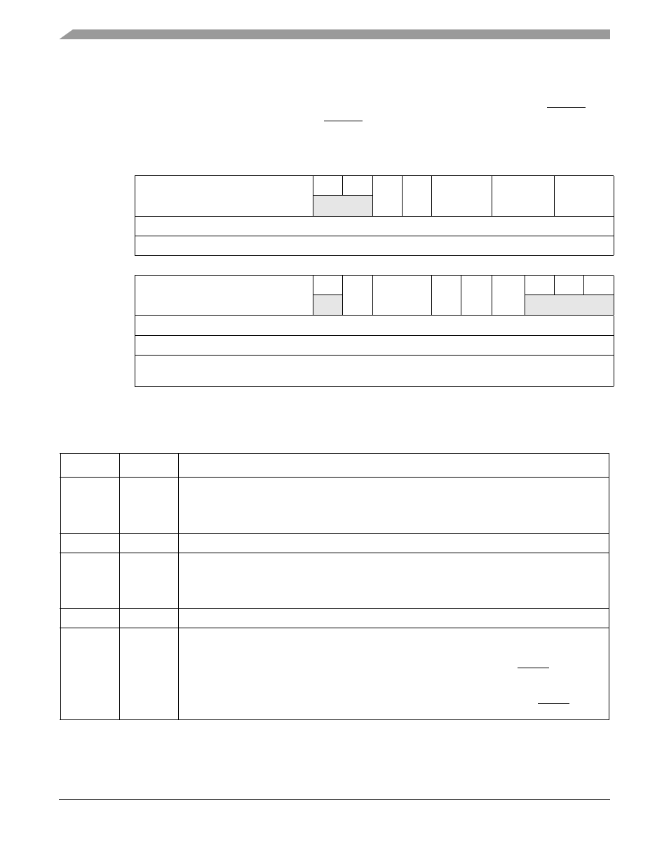
Chip-Select Control Registers (CSCR0–CSCR5)
Each CSCRn,
, controls the auto acknowledge, address setup and hold times, port size, burst
capability, and activation of each chip-select. Note that to support the global chip-select, FBCS0, the
CSCR0 reset values differ from the other CSCRs. FBCS0 allows address decoding for boot ROM before
system initialization.
describes CSCRn fields.
31
30
29
28
27
26
25
24
23
22
21
20
19
18
17
16
R
SWS
0
0
SWS
EN
—
ASET
RDAH
WRAH
W
Reset: CSCR0
0
0
0
0
0
0
0
0
0
0
1
1
1
1
1
1
Reset: CSCRs
0
0
0
0
0
0
0
0
0
0
0
0
0
0
0
0
15
14
13
12
11
10
9
8
7
6
5
4
3
2
1
0
R
WS
0
AA
PS
BEM BSTR BSTW
0
0
0
W
Reset: CSCR0
1
1
1
1
1
1
0
AD2
AD[1:0]
AD3
0
0
0
0
0
Reset: CSCRs
0
0
0
0
0
0
0
0
0
0
0
0
0
0
0
0
Reg
Addr
MBAR + 0x508 (CSCR0); 0x514 (CSCR1); 0x520 (CSCR2);
0x52C (CSCR3); 0x538 (CSCR4); 0x544 (CSCR5)
Figure 17-5. Chip-Select Control Registers (CSCRn)
Table 17-9. CSCRn Field Descriptions
Bits
Name
Description
31–26
SWS
Secondary wait states. The number of wait states inserted before an internal transfer acknowledge
is generated for burst transfer except for the first termination, which is controlled by the wait state
count. The secondary wait state is only used if the secondary wait state enable is set, otherwise the
wait state value is used for all burst transfers.
25–24
—
Reserved, should be cleared
23
SWSEN
Secondary wait state enable. If set (SWSEN = 1), then the secondary wait state value is used to
insert wait states before an internal transfer acknowledge is generated for burst transfer secondary
terminations. If cleared (SWSEN = 0), then the wait state value is used to insert wait states before
an internal transfer acknowledge is generated for all transfers.
22
—
Reserved, should be cleared
21–20
ASET
Address setup. This field controls the asserting of chip-select with respect to assertion of a valid
address and attributes. Note that the address and attributes are considered valid at the same time
ALE asserts.
00 Assert chip-select on rising clock edge after address is asserted. (Default FBCSn)
01 Assert chip-select on second rising clock edge after address is asserted.
10 Assert chip-select on third rising clock edge after address is asserted.
11 Assert chip-select on fourth rising clock edge after address is asserted.(Reset FBCS0)