3 base address register overview – Freescale Semiconductor MCF5480 User Manual
Page 558
MCF548x Reference Manual, Rev. 3
19-74
Freescale Semiconductor
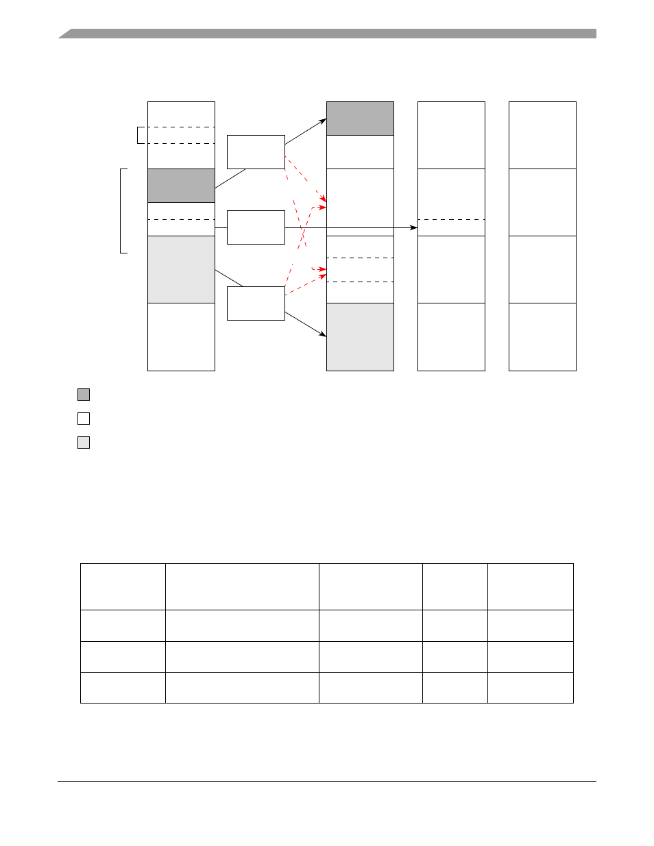
Figure 19-55. Outbound Address Map
19.5.2.1.3
Base Address Register Overview
shows the available accessibility for all PCI associated base address and translation address
registers in the MCF548x.
Table 19-58. Address Register Accessibility
Base Address
Register
Register Function
PCI Bus
Configuration
Access
Processor
Access
Any XL Bus
Master Access
BAR0
PCI Base Address Register 0
(256 Kbyte)
X
X
X
BAR1
PCI Base Address Register 1
(1 Gbyte)
X
X
X
TBATR0
Target Base Address Translation
Register 0 (256 Kbyte)
X
X
0
4G
Register Space
3G
2G
1G
PCI Space
Window 2
XLB
Initiator
Windows
0
4G
3G
2G
1G
0
4G
3G
2G
1G
0
4G
3G
2G
1G
MCF548X
Window 2
Window 0
Window 0
Window 0
Translation
Window 1
MBAR
Window 1
Translation
Window 1
Not Recommended
Window 2
Translation
Not Recommended
Window 2 Base Address = 0x80
Window 2 Address Mask = 0x3F
Window 2 Translation Address = 0xC0
Window 0 Base Address = 0x40
Window 0 Address Mask = 0x1F
Window 0 Translation Address = 0x00
Associated with PCI
Prefetchable Memory
Window 1 Base Address = 0x70
Window 1 Address Mask = 0x0F
Window 1 Translation Address = 0x70
Associated with PCI
Non-Prefetchable Memory
Associated with PCI I/O
(Memory View)
PCI Space
(I/O View)
(Configuration
View)
MCF548X
Memory
Memory
MCF548x Space