4 external request module registers, 1 external request module register map, 2 external request base address register (ereqbar) – Freescale Semiconductor MCF5480 User Manual
Page 740: External request module registers -20, External request module register map -20, Table 24-18/24-20
MCF548x Reference Manual, Rev. 3
24-20
Freescale Semiconductor
24.3.4
External Request Module Registers
The following section shows the registers contained within the multichannel DMA external request
module. Details are given regarding register mapping, programming notes, bit definitions, and operating
modes.
24.3.4.1
External Request Module Register Map
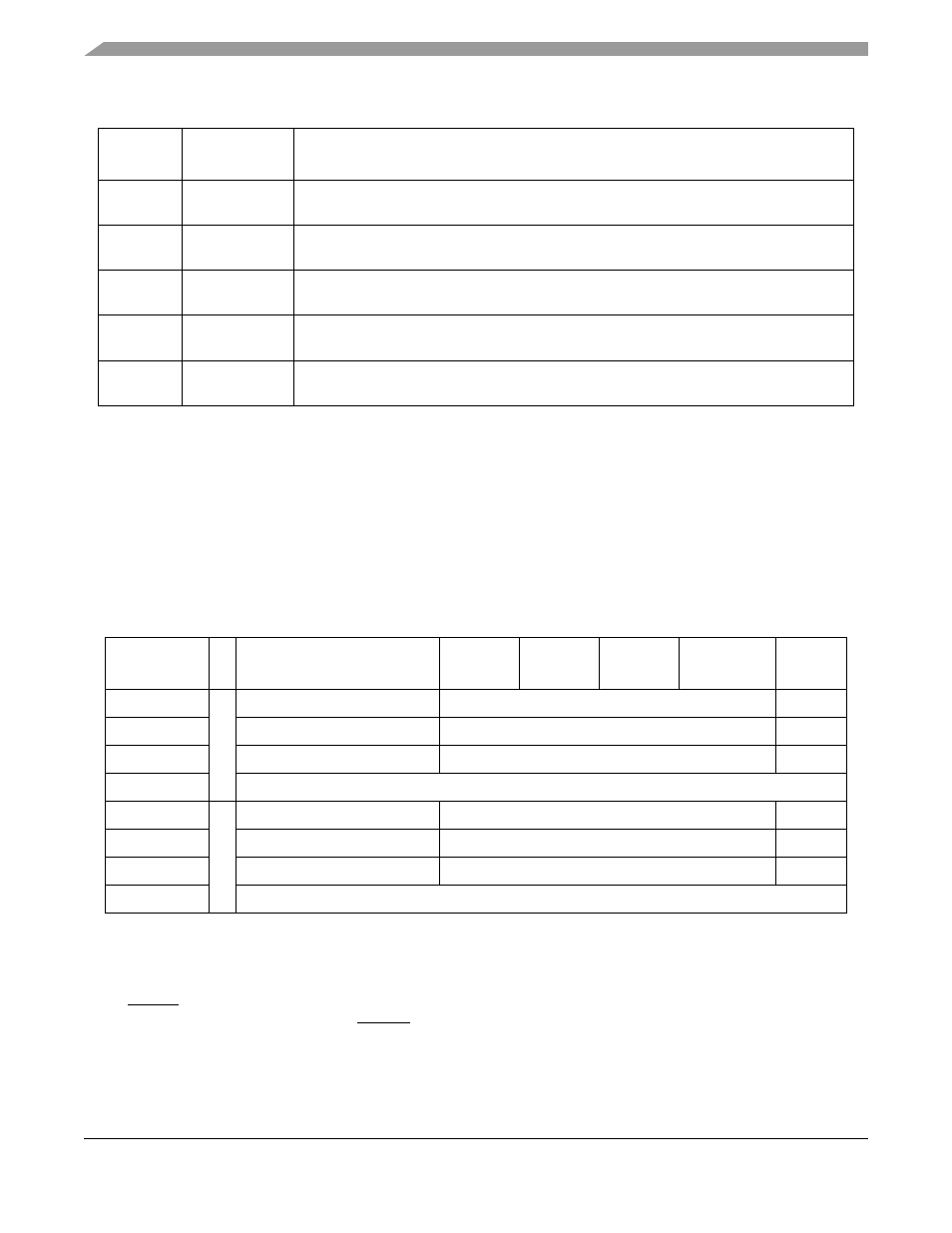
The following table shows the register mapping of the external request module.
Because each channel contains the same set of registers, only one set of registers will be defined.
24.3.4.2
External Request Base Address Register (EREQBAR)
After DREQ is asserted, this register contains an address value used for the compare that determines a hit
for the external acknowledge signal, DACK. This address value can be valid for comm bus cycles, system
SRAM, external memory, or comm bus peripherals. This register can be read or written at any time. The
reset state of this register is set to all zeros.
4
taskEnable
PTDDBG[15:0] reflects the state of the EN (task enable) bit in each of the Task Control
Registers (TCRs).
5
taskRun
PTDDBG[15:0] reflects whether the corresponding task is enabled, valid and not blocked
by the debug module.
6
dbgTaskBlock
PTDDBG[15:0] reflects the state of the Task Blocked field of the Debug Status register
(DBGSTAT).
7
alwaysInit
PTDDBG[15:0] reflects the state of the ALWINIT bit in each of the Task Control Registers
(TCRs).
8
taskStart
PTDDBG[15:0] reflects the state of the Auto-start (ASTRT) bit in each task’s control
register (TCR).
Table 24-18. External Request Module Register Mapping
Address
(MBAR +)
Name
Byte0
Byte1
Byte2
Byte3
Access
0x0D00
Initia
to
r 1
Base Address Register 0
EREQBAR0
R/W
0x0D04
Base Address Mask Register 0
EREQMASK0
R/W
0x0D08
Control Reg 0
EREQCTRL0
R/W
0x0D0C
Reserved
0x0D10
Initia
tor 2
Base Address Register 1
EREQBAR1
R/W
0x0D14
Base Address Mask Register 1
EREQMASK1
R/W
0x0D18
Control Reg 1
EREQCTRL1
R/W
0x0D1C
Reserved
Table 24-17. PTD Debug Register Descriptions (Continued)
Value
Written
Reg Name
Description