Psctfdrn), This register applies to all modes – Freescale Semiconductor MCF5480 User Manual
Page 789
Memory Map/Register Definition
MCF548x Reference Manual, Rev. 3
Freescale Semiconductor
26-27
26.3.3.21 Rx and Tx FIFO Counter Register (PSCRFCNTn, PSCTFCNTn)
This register applies to all modes.
26.3.3.22 Rx and Tx FIFO Data Register (PSCRFDRn, PSCTFDRn)
These registers provide access to the internal Rx and Tx FIFOs.
Table 26-27. PSCIRFDRn Field Descriptions
Bits
Name
Description
7–4
—
Reserved, should be cleared.
3–0
F_FDIV
Applies only in FIR mode; in all other modes, this field is reserved.
In FIR mode, this field signifies clock divide ratio.
The bit frequency is derived by the following equation.
Eqn. 26-2
This bit frequency should be 8 MHz. In order to receive the minimum pulse width described in the
IrDA spec, (F_FDIV + 1) should be larger than or equal to 4. shows several frequency selection.
See
Table 26-28., “Frequency Selection in FIR Mode
Table 26-28. Frequency Selection in FIR Mode
F_FDIV[3:0]
Frequency of bit_clk [MHz]
3
32.0
4
40.0
5
48.0
6
56.0
...
...
15
14
13
12
11
10
9
8
7
6
5
4
3
2
1
0
R
0
0
0
0
0
0
0
CNT
W
Reset
0
0
0
0
0
0
0
0
0
0
0
0
0
0
0
0
Reg
Addr
MBAR + 0x8658 (PSCRFCNT0); 0x8758 (PSCRFCNT1); 0x8858 (PSCRFCNT2); 0x8958 (PSCRFCNT3)
and MBAR + 0x865C (PSCTFCNT0); 0x875C (PSCTFCNT1); 0x885C (PSCTFCNT2); 0x895C (PSCTFCNT3)
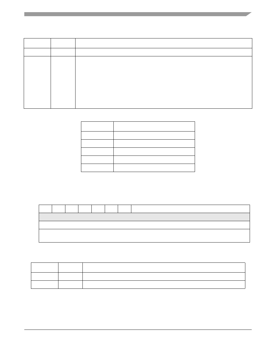
Figure 26-18. RxFIFO (PSCRFCNTn) and TxFIFO (PSCTFCNTn) Counter Register
Table 26-29. PSCRFCNTn and PSCTFCNTn Field Descriptions
Bits
Name
Description
15-9
—
Reserved, should be cleared.
8–0
CNT
Number of bytes in the FIFO
f
bit
f
bit_clk
F_FDIV 1
+
------------------------------
=