1 system sram configuration register (sscr), System sram configuration register (sscr) -3 – Freescale Semiconductor MCF5480 User Manual
Page 411
Memory Map/Register Definition
MCF548x Reference Manual, Rev. 3
Freescale Semiconductor
16-3
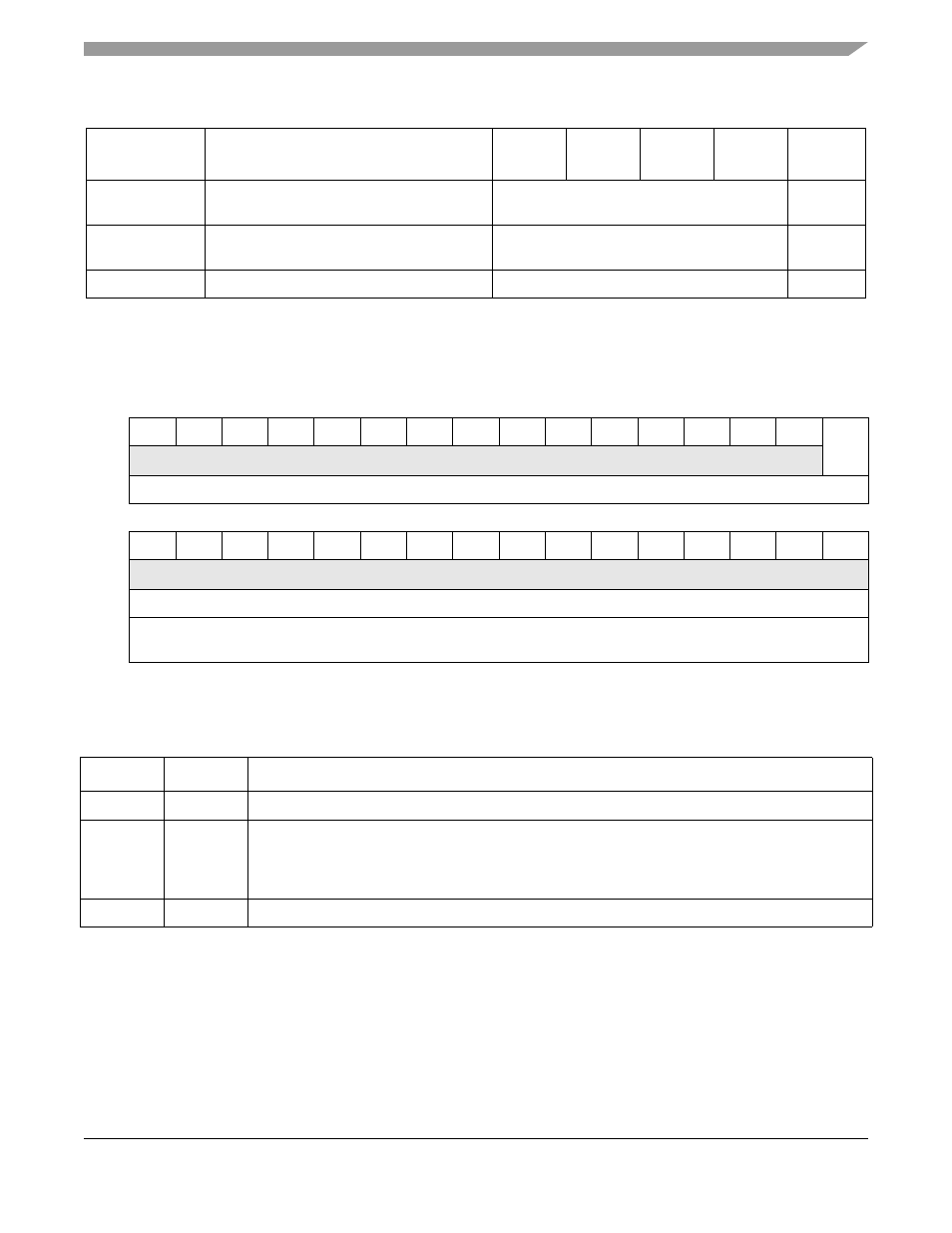
16.2.1
System SRAM Configuration Register (SSCR)
This register is used to define the base address of the system SRAM and whether to interleave the banks.
Each field is described in
.
0x1_FFCC
Transfer Count Configuration Register - DMA
Write Channel
TCCRDW
R/W
0x1_FFD0
Transfer Count Configuration Register - SEC
TCCRSEC
R/W
31
30
29
28
27
26
25
24
23
22
21
20
19
18
17
16
R
0
0
0
0
0
0
0
0
0
0
0
0
0
0
0
INLV
W
Reset
0
0
0
0
0
0
0
0
0
0
0
0
0
0
0
0
15
14
13
12
11
10
9
8
7
6
5
4
3
2
1
0
R
0
0
0
0
0
0
0
0
0
0
0
0
0
0
0
0
W
Reset
0
0
0
0
0
0
0
0
0
0
0
0
0
0
0
0
Reg
Addr
MBAR + 0x1_FFC0
Figure 16-2. System SRAM Configuration Register (SSCR)
Table 16-2. SSCR Register Field Descriptions
Bits
Name Description
31–17
—
Reserved, should be cleared.
16
INLV
Interleave enable. Controls whether the banks are interleaved along longword boundaries or linear.
0 The four SRAM banks are not interleaved (linear).
1 The four SRAM banks are interleaved. SRAM bank # contains data for long word address modulo
{bank #}
15–0
—
Reserved. Should be cleared.
Table 16-1. System SRAM Memory Map (Continued)
Address
(MBAR + )
Name
Byte 0
Byte 1
Byte 2
Byte 3
Access
0x1_0000–
0x1_7FFC
SRAM Contents
R/W