2 chip-select registers, Chip-select registers -7, Table 17-4 – Freescale Semiconductor MCF5480 User Manual
Page 423: Table 17-5
Chip-Select Operation
MCF548x Reference Manual, Rev. 3
Freescale Semiconductor
17-7
17.5.2
Chip-Select Registers
The following tables describe in detail the registers and bit meanings for configuring chip-select operation.
The chip-select controller register map is accessed relative to the memory base address register (MBAR).
shows the chip-select register memory map. Reading unused or reserved locations terminates
normally and returns zeros.
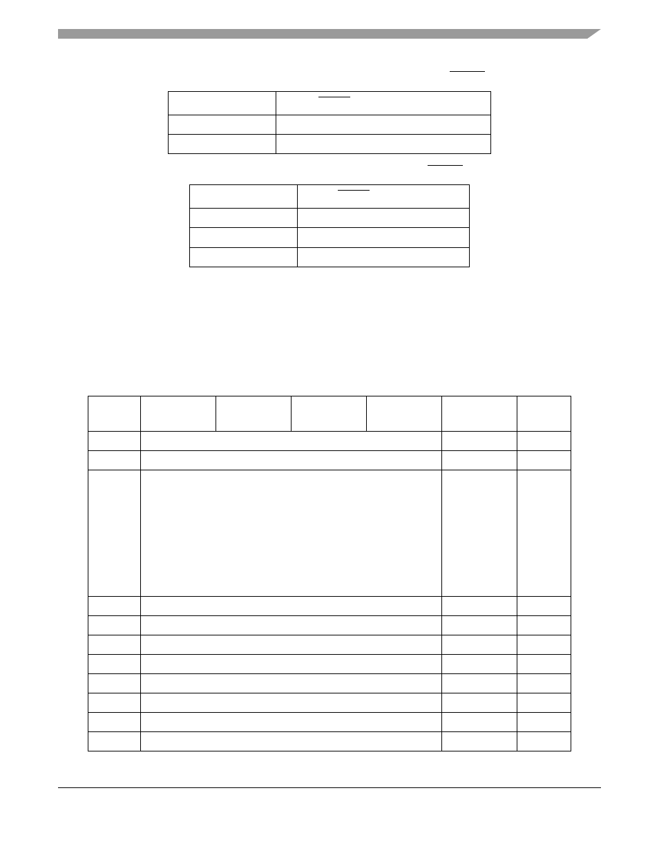
Table 17-4. AD[2]/AA Automatic Acknowledge of Boot FBCS0
AD[2]/AA
Boot FBCS0 AA Configuration at Reset
0
Disabled
1
Enabled with 63 wait states
Table 17-5. AD[1:0]/PS[1:0], Port Size of Boot FBCS0
AD[1:0]/PS[1:0]
Boot FBCS0 Port Size at Reset
00
32-bit port
01
8-bit port
1x
16-bit port
Table 17-6. Chip-Select Registers
Register
Offset
[31:24]
[23:16]
[15:8]
[7:0]
ResetValue
Access
1
0x0500
Chip-select address register—bank 0 (CSAR0)
0x0000_0000
R/W
0x0504
Chip-select mask register—bank 0 (CSMR0)
0x0000_0000
R/W
0x0508
Chip-select control register—bank 0 (CSCR0)
BSTW = 0
BSTR = 0
PS = AD[1:0]
AA = AD[2]
WS = 111111
WRAH = 11
RDAH = 11
ASET = 11
SWSEN = 0
SWS = 000000
R/W
0x050C
Chip-select address register—bank 1 (CSAR1)
0x0000_0000
R/W
0x0510
Chip-select mask register—bank 1 (CSMR1)
0x0000_0000
R/W
0x054
Chip-select control register—bank 1 (CSCR1)
0x0000_0000
R/W
0x0518
Chip-select address register—bank 2 (CSAR2)
0x0000_0000
R/W
0x051C
Chip-select mask register—bank 2 (CSMR2)
0x0000_0000
R/W
0x0520
Chip-select control register—bank 2 (CSCR2)
0x0000_0000
R/W
0x0524
Chip-select address register—bank 3 (CSAR3)
0x0000_0000
R/W
0x0528
Chip-select mask register—bank 3 (CSMR3)
0x0000_0000
R/W