2 external signal description, 1 address/data bus (pciad[31:0]), 2 command/byte enables (pcicxbe[3:0]) – Freescale Semiconductor MCF5480 User Manual
Page 486: External signal description -2, Address/data bus (pciad[31:0]) -2, Command/byte enables (pcicxbe[3:0]) -2
MCF548x Reference Manual, Rev. 3
19-2
Freescale Semiconductor
•
Compatible with PCI 2.2 specification
•
PCI initiator and target operation
•
Fully synchronous design
•
32-bit PCI address bus
•
PCI 2.2 Type 0 configuration space header
•
Supports the PCI 16/8 clock rule
•
PCI master multichannel DMA or CPU access to PCI bus
•
Ideal transfer rates up to 266 Mbytes/sec. (66 MHz clock, 128 byte buffer)
•
PCI to system bus address translation
•
Target response is medium DEVSEL generation
•
Initiator latency time-outs
•
Automatic retry of target disconnects
19.2
External Signal Description
For detailed description of the PCI bus signals, see the PCI Local Bus Specification, Revision 2.2.
19.2.1
Address/Data Bus (PCIAD[31:0])
The PCIAD[31:0] lines are a time multiplexed address data bus. The address is presented on the bus during
the address phase while the data is presented on the bus during one or more data phases.
19.2.2
Command/Byte Enables (PCICXBE[3:0])
The PCICXBE[3:0] lines are time multiplexed. The PCI command is presented during the address phase
and the byte enables are presented during the data phase. Byte enables are active low.
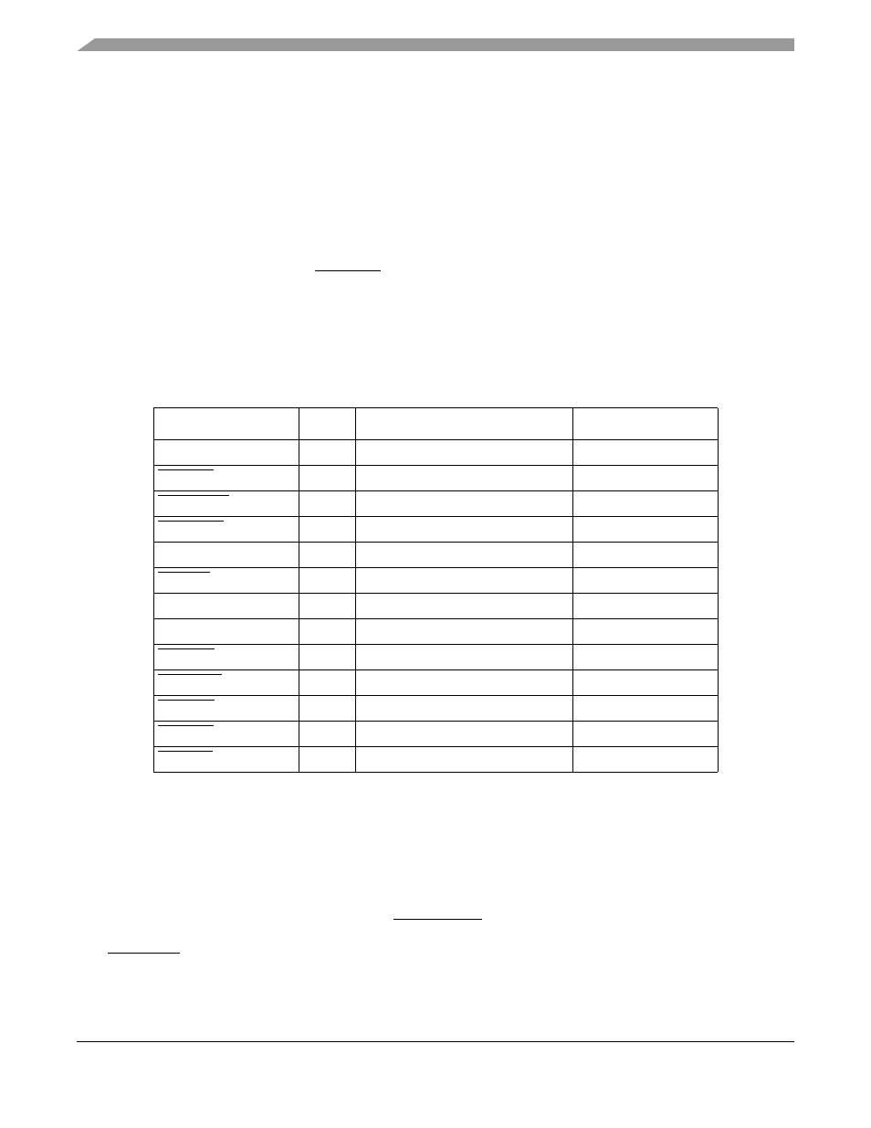
Table 19-1. PCI Module External Signals
Name
Type
Function
MCF548x Reset
PCIAD[31:0]
I/O
PCI Address Data Bus
Tristate
PCICXBE[3:0]
I/O
PCI Command/Bytes Enables
Tristate
PCIDEVSEL
I/O
PCI Device Select
Tristate
PCIFRAME
I/O
PCI Frame
Tristate
PCIIDSEL
I
PCI Initialization Device Select
Tristate
PCIIRDY
I/O
PCI Initiator Ready
Tristate
PCIPAR
I/O
PCI Parity
Tristate
CLKIN
I
PCI Clock
Toggling
PCIPERR
I/O
PCI Parity Error
Tristate
PCIRESET
O
PCI Reset
0
PCISERR
I/O
PCI System Error
Tristate
PCISTOP
I/O
PCI Stop
Tristate
PCITRDY
I/O
PCI Target Ready
Tristate