Freescale Semiconductor MCF5480 User Manual
Page 394
MCF548x Reference Manual, Rev. 3
15-22
Freescale Semiconductor
15.3.2.6
FlexBus Chip Select Pin Assignment Register (PAR_FBCS)
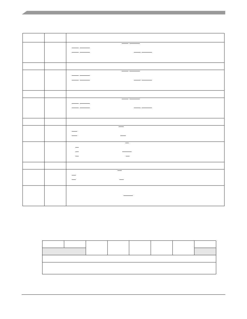
The PAR_FBCS register controls the function of the FlexBus chip select signal pins. The PAR_FBCS
register is read/write.
12
PAR_BWE2 The PAR_BWE bit configures the BE2/BWE2 pin for its primary function or general purpose I/O.
0 BE2/BWE2 pin configured for general purpose I/O (PFBCTL6)
1 BE2/BWE2 pin configured for FlexBus BE2/BWE2 or TSIZ0 function.
The function chosen depends on the reset configuration.
11
—
Reserved, should be cleared. Writes have no effect and terminate without transfer error exception
10
PAR_BWE1 The PAR_BWE bit configures the BE1/BWE1 pin for its primary function or general purpose I/O.
0 BE1/BWE1 pin configured for general purpose I/O (PFBCTL5)
1 BE1/BWE1 pin configured for FlexBus BE1/BWE1 or FBADDR1 function.
The function chosen depends on the reset configuration.
9
—
Reserved, should be cleared.
8
PAR_BWE0 The PAR_BWE bit configures the BE0/BWE0 pin for its primary function or general purpose I/O.
0 BE0/BWE0 pin configured for general purpose I/O (PFBCTL4)
1 BE0/BWE0 pin configured for FlexBus BE0/BWE0 or FBADDR0 function.
The function chosen depends on the reset configuration.
7
—
Reserved, should be cleared.
6
PAR_OE
The PAR_OE bit configures the OE pin for its primary function or general purpose I/O.
0 OE pin configured for general purpose I/O (PFBCTL3)
1 OE pin configured for Flexbus OE function.
5–4
PAR_RWB
The PAR_RWB bit configures the R/W pin for its primary function or general purpose I/O
0x R/W pin configured for general purpose I/O (PFBCTL2)
10R/W pin configured for Flexbus TBST function
11R/W pin configured for Flexbus R/W function
3
—
Reserved, should be cleared.
2
PAR_TA
The PAR_TA bit configures the TA pin for its primary function or general purpose I/O
0 TA pin configured for general purpose I/O (PFBCTL1)
1 TA pin configured for Flexbus TA function
1–0
PAR_ALE
The PAR_ALE bit configures the ALE pin for one of its primary functions or general purpose I/O.
0X ALE pin configured for general purpose I/O (PFBCTL0)
10 ALE pin configured for Flexbus TBST function
11 ALE pin configured for Flexbus ALE function
7
6
5
4
3
2
1
0
R
0
0
PAR_CS5
PAR_CS4
PAR_CS3
PAR_CS2
PAR_CS1
0
W
Reset
0
0
1
1
1
1
1
0
Reg
Addr
MBAR + 0xA42 (PAR_FBCS)
Figure 15-23. Flexbus Chip Select Pin Assignment Register (PAR_FBCS)
Table 15-24. PAR_FBCTL Field Descriptions (Continued)
Bits
Name Description