4 sdram row address strobe (ras), 5 sdram column address strobe (cas), 6 sdram chip selects (sdcs[3:0]) – Freescale Semiconductor MCF5480 User Manual
Page 451: 7 sdram write data byte mask (sddm[3:0]), 8 sdram data strobe (sddqs[3:0]), 9 sdram clock (sdclk[1:0]), 10 inverted sdram clock (sdclk[1:0]), 11 sdram write enable (sdwe), Sdram row address strobe (ras, Sdram column address strobe (cas
External Signal Description
MCF548x Reference Manual, Rev. 3
Freescale Semiconductor
18-3
18.3.4
SDRAM Row Address Strobe (RAS)
This output is the SDRAM synchronous row address strobe.
18.3.5
SDRAM Column Address Strobe (CAS)
This output is the SDRAM synchronous column address strobe.
18.3.6
SDRAM Chip Selects (SDCS[3:0])
These signals interface to the chip select lines of the SDRAMs within a memory block. Thus, there is one
SDCS line for each memory block (the MCF548x supports up to four SDRAM memory blocks).
18.3.7
SDRAM Write Data Byte Mask (SDDM[3:0])
These output signals are sampled by the SDRAM on both edges of SDDQS to determine which byte lanes
of the SDRAM data bus should be latched during a write cycle. In DDR mode, these bits are ignored during
read operations.
18.3.8
SDRAM Data Strobe (SDDQS[3:0])
These bidirectional signals indicate when valid data is on the SDRAM data bus.
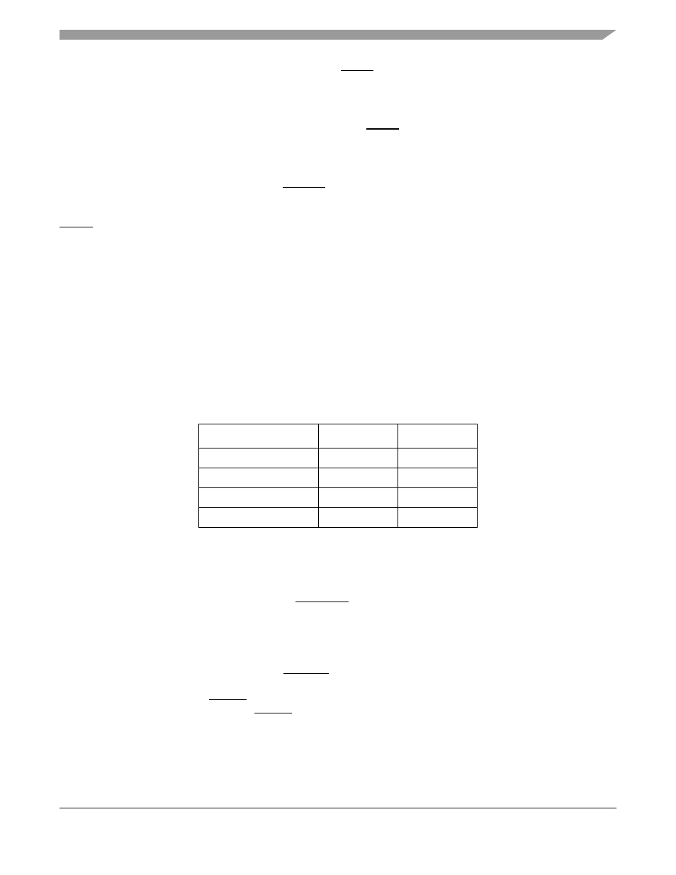
correspondence between SDDATA byte lanes and the SDDQS and SDDM signals.
18.3.9
SDRAM Clock (SDCLK[1:0])
This is the output clock for SDRAM accesses.
18.3.10 Inverted SDRAM Clock (SDCLK[1:0])
This is the inverted version of the SDRAM clock. It is used with SDCLK to provide the differential clocks
for DDR SDRAM.
18.3.11 SDRAM Write Enable (SDWE)
The SDRAM write enable (SDWE) is asserted to signify that a DRAM write cycle is underway. A read
cycle is indicated by the negation of SDWE.
Table 18-1. SDDQS and SDDM to Byte Lane Mapping
Byte Lane
SDDQS
SDDM
SDDATA[31:24] (MSB)
SDDQS3
SDDM3
SDDATA[23:16]
SDDQS2
SDDM2
SDDATA[15:8]
SDDQS1
SDDM1
SDDATA[7:0] (LSB)
SDDQS0
SDDM0