3 block diagram, 3 external signal description, 1 sdram data bus (sddata[31:0]) – Freescale Semiconductor MCF5480 User Manual
Page 450: 2 sdram address bus (sdaddr[12:0]), 3 sdram bank addresses (sdba[1:0]), Block diagram -2, External signal description -2, Sdram data bus (sddata[31:0]) -2, Sdram address bus (sdaddr[12:0]) -2, Sdram bank addresses (sdba[1:0]) -2
MCF548x Reference Manual, Rev. 3
18-2
Freescale Semiconductor
18.2.3
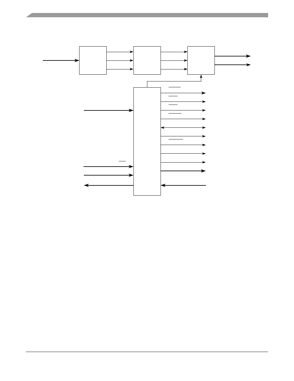
Block Diagram
Figure 18-1. SDRAM Controller Block Diagram
18.3
External Signal Description
18.3.1
SDRAM Data Bus (SDDATA[31:0])
SDDATA[31:0] is the bidirectional, non-multiplexed data bus used for SDRAM accesses. Data is sampled
by the MCF548x on the rising edge of SDCLK when in SDR mode, and on both the rising and falling edge
of SDCLK when in DDR mode.
18.3.2
SDRAM Address Bus (SDADDR[12:0])
The SDADDR[12:0] signals are the 13-bit, uni-directional address bus used for multiplexed row and
column addresses during SDRAM bus cycles. The address multiplexing supports up to 256 Mbytes of
SDRAM per chip select.
18.3.3
SDRAM Bank Addresses (SDBA[1:0])
Each SDRAM module has four internal row banks. The SDBA[1:0] signals are used to select the row bank.
It is also used to select the SDRAM internal mode register during power-up initialization.
addr[1:3]
CAS
SDWE
SDDQS
SDCLK[1:0]
SDCLK[1:0]
SDCKE
RAS
SDCS[3:0]
dataout[63:0]
SDDM
SDDATA[31:0]
SDDATA[31:0]
Row
Bank
Column
addr[29:4]
Row
Bank
Column
SDBA[1:0]
SDADDR[12:0]
Select
datain[63:0]
SDRAM
Controller
State
Machine
Read Data
Buffer
Write Data
Buffer
Address
Output
MUX
Address
Pipeline
Latches
Address
Input
MUX
tsiz[1:0], tbst