6 sdram configuration register 2 (sdcfg2), Sdram configuration register 2 (sdcfg2) -23 – Freescale Semiconductor MCF5480 User Manual
Page 471
Memory Map/Register Definition
MCF548x Reference Manual, Rev. 3
Freescale Semiconductor
18-23
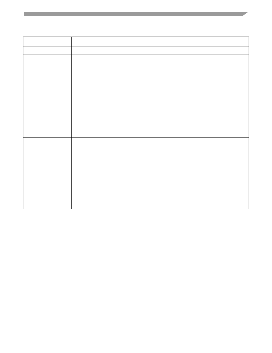
18.7.6
SDRAM Configuration Register 2 (SDCFG2)
The 32-bit read/write configuration register 2 stores delay values necessary between specific SDRAM
commands. During initialization, software loads values to the register according to the SDRAM
information obtained from the data sheet. This register is reset only by a power-up reset signal.
The burst length (BL) field must be exact. All other fields govern the relative timing from one command
to another, they have minimum values, but any larger value is also legal (but with decreased performance).
All delays in this register are expressed in SDCLK.
19
—
Reserved. Should be cleared.
18–16
ACT2RW
Active to Read/Write delay. Active command to any following read or write delay counter.
Suggested value = t
RCD
/SDCLK - 1 (Round up to nearest integer)
EXAMPLE:
If t
RCD
= 20ns and SDCLK = 99 MHz
20ns / 10.1 ns = 1.98; round to 2; write 0x1.
Note: Count value is in SDCLK periods for both SDR and DDR mode.
15
—
Reserved. Should be cleared.
14–12
PRE2ACT
Precharge to Active delay. Precharge command to following Active command delay counter.
Suggested value = t
RP
/SDCLK - 1 (Round up to nearest integer)
EXAMPLE:
If t
RP
= 20ns and SDCLK = 99MHz
20ns / 10.1ns = 1.98; round to 2; write 0x1.
Note: Count value is in SDCLK periods for both SDR and DDR mode.
11–8
REF2ACT
Refresh to Active delay. Refresh command to following Active or Refresh command delay counter.
Suggested value = t
RFC
/SDCLK - 1 (Round up to nearest integer)
EXAMPLE:
If t
RFC
= 75ns and SDCLK = 99MHz
75ns / 10.1ns = 7.425; round to 8; write 0x7.
Note: Count value is in SDCLK periods for both SDR and DDR mode.
7
—
Reserved. Should be cleared.
6–4
WTLAT
Write latency. Write command to write data delay counter.
For DDR, write 0x3
For SDR, write 0x0
3–0
—
Reserved. Should be cleared.
Table 18-12. SDCFG1 Field Descriptions (Continued)
Bits
Name Description